
Buyers ask when to use X-ray inspection on a PCBA when AOI and visual checks stop seeing the joints that matter. The useful answer is not “always X-ray every board” or “X-ray is nicer optics.” It is a decision guide: which packages force hidden-joint review, what void and bridge criteria belong in writing, when 2D is enough versus 3D AXI, how sampling scales with risk and volume, and what China fab RFQ language locks coverage, accept limits, and image retention.
This page stays on the buyer gate — when to require X-ray / AXI — not a service menu of machines, not a reflow-profile deep dive, and not a full testing-methods encyclopedia. Those jobs need their own travelers. Here the goal is shared language so procurement and manufacturing engineering mandate inspection where risk lives and skip theater where it does not.
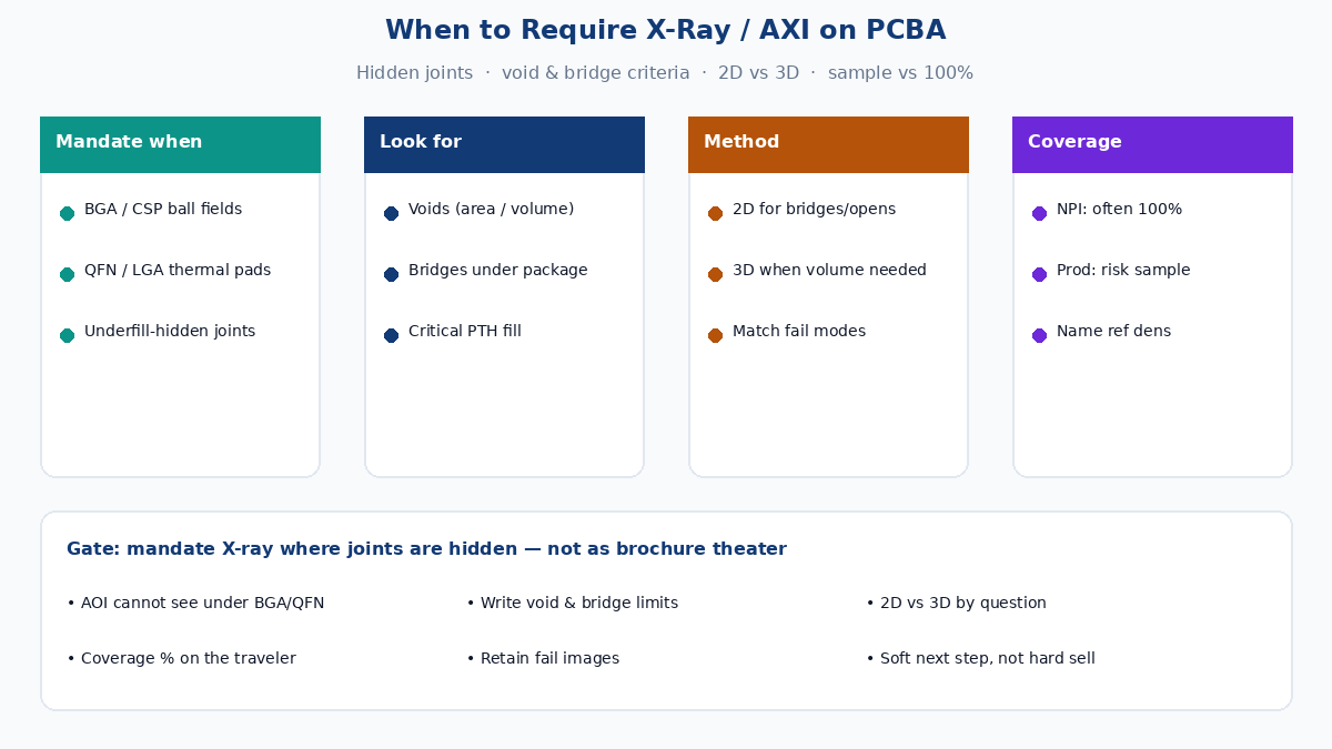
What X-ray adds that AOI and visual cannot
AOI and human visual inspection see topside lands, polarity, missing parts, and many open soldering defects on gull-wing and chip packages. They cannot see under a BGA ball field, under a QFN / LGA thermal pad, inside a CSP array, or through solder that fills a plated through-hole. X-ray (radiography) images density differences: solder, voids, bridges, and missing fill show as contrast against copper and laminate.
Factory talk usually splits two tool families:
2D X-ray. Transmission image from one viewing angle (sometimes with tilt). Fast enough for high sample rates or 100% on critical packages. Good for gross opens, bridges under packages, major misalignment, and area-style void estimates on a ball field.
3D / AXI (automated X-ray inspection) with tomography or multi-angle reconstruction. Slower and more expensive per board, but better when stacked voids, complex packages, or volume void % need more than a flat shadow. Treat 3D as a deeper method for selected lots or first articles — not as a synonym for “any X-ray photo.”
Neither replaces electrical test, SPI paste check, or functional coverage. X-ray answers “is the hidden joint geometrically acceptable?” It does not prove the firmware boots.
Package and joint types that force the mandate
Require X-ray when the acceptance-critical joint is hidden or only partially visible.
BGA and CSP ball fields. Optical cameras see the package body, not the solder balls. Opens, bridges between balls, head-in-pillow class non-wets, and large voids hide under the package. If the BOM carries fine-pitch BGA / CSP and the quality plan cares about those nets, X-ray belongs on the traveler — not as an optional souvenir photo.
QFN, LGA, and other bottom-terminated packages. Center thermal pads and perimeter lands under the body are classic failure sites for voids and bridges. AOI may catch toe fillet on some QFN designs; it will not certify the pad under the package.
Underfill and overmold situations. After underfill, visual access collapses further. Decide whether X-ray of the solder joint happens before underfill, or whether post-underfill review is still required for specific defects — write the sequence so the shop does not skip the only window that still works.
Hidden interconnect beyond packages. Press-fit barrels, connector solder tails buried in housings, and dense double-sided SMT where one side shadows the other can also justify X-ray. Name the parts on the assembly drawing; “X-ray available” without a callout is how coverage becomes random.
When you can skip a hard mandate. Coarse SMT with fully visible fillets, through-hole parts whose topside and bottomside fillets are visually inspectable, and low-risk consumer prototypes with no BGA/QFN often stay on AOI + visual + electrical test. Adding X-ray “because it sounds thorough” burns schedule and money without changing escape risk.
Defect modes: voids, bridges, PTH fill
Name the defects you will fail — vague “check soldering” language produces pretty images and soft dispositions.
Solder voids. Gas or flux entrapment leaves cavities in the joint. Power packages and QFN thermal pads often need stricter area limits than signal balls because voids cut thermal and current paths. Decide whether the limit is total void area %, largest single void, or both, and whether measurement is 2D projection or 3D volume. Put the number and method on the quality plan; do not invent a universal percentage as a plant promise.
Bridges under packages. Excess paste, placement offset, or warpage can short adjacent balls or QFN lands where no camera reaches. 2D X-ray with appropriate contrast and magnification is the workhorse for catching these before ICT or functional test spends hours chasing intermittent shorts.
PTH / pin-hole fill. Wave or selective solder joints that must meet fill height or wetting criteria inside the barrel are hard to judge from one visible fillet alone. X-ray (or microsection on coupons) confirms fill where Class or customer notes demand it. Call out which holes are critical — power pins, connector rows, thermal vias used as solder paths — so the shop does not X-ray every barrel on a dense board.
Opens and misalignment. Missing balls, major pad offset, and non-collapse joints show as density gaps or geometry errors. Pair X-ray disposition with process notes (paste, VIP fill, profile ownership) so the fix is not “take another photo.”
Criteria that belong on paper. For BGA signal balls, many programs start with a documented area-void cap and a hard fail on bridge or missing ball. For QFN / power thermal pads, tighten the void rule and state whether the whole pad is one measurement zone. For PTH, state minimum fill height or wetting class language your drawing already uses — X-ray then verifies the barrel, it does not invent a new standard. If industry handbooks or customer specs already name a void band for your product class, cite that document on the PO; do not rely on tribal memory at the programming station.
2D vs 3D AXI — choose by question, not by brochure
| Question you need answered | Practical choice |
|---|---|
| Bridges, gross opens, ball presence under BGA/QFN | 2D X-ray, often enough for production gate |
| Area void % on thermal pads with clear projection | 2D with agreed measurement method |
| Stacked / overlapping void volume, complex package stack | 3D / CT-class AXI on sample or FA |
| High volume, repetitive footprint, known process window | 2D AXI automation or high-rate 2D sampling |
| First article on a new fine-pitch BGA | 100% 2D on critical packages; add 3D if void debate needs volume |
Buyers who write only “3D X-ray” on every RFQ pay for reconstruction time they may not use. Buyers who write only “X-ray photo OK” get a JPEG with no accept criteria. Match method to the defect you will scrap on.
Sampling vs 100% — risk and volume drive coverage
Coverage is a quality-plan number, not a moral slogan.
First article / NPI. Many programs run 100% X-ray on all BGA/QFN (and other called-out parts) for the first article lot, or until the process window is proven. That is where you catch paste, VIP, and profile mistakes before volume commits.
Ongoing production. After yield stabilizes, switch to a documented sample plan: every nth board, every lot with a fixed sample size, or tightened sampling after a process change (stencil, paste lot, profile tweak, new feeder setup). High-reliability or safety-critical builds may keep 100% on hidden joints for the life of the product — say so explicitly.
Risk triggers that push coverage up. Fine pitch, high ball count, power thermal pads, history of void escapes, new package MPN, double-sided reflow with heavy copper, or customer audits that ask for retained images. Risk triggers that allow coverage down: mature process, coarse pitch, strong SPI+AOI upstream, and electrical coverage that catches the same failure modes.
Write both the percentage (or AQL-style sample) and the unit of coverage: “100% of BGA U12/U14 balls on every board” is executable; “some X-ray” is not.
Rework and re-inspection. If a failed joint is reworked, decide whether that serial number returns to X-ray before ship. Skipping re-X-ray after BGA rework is a common escape path. Put the rule next to the coverage table so operators are not guessing at pack-out.
China PCBA RFQ language that locks the gate
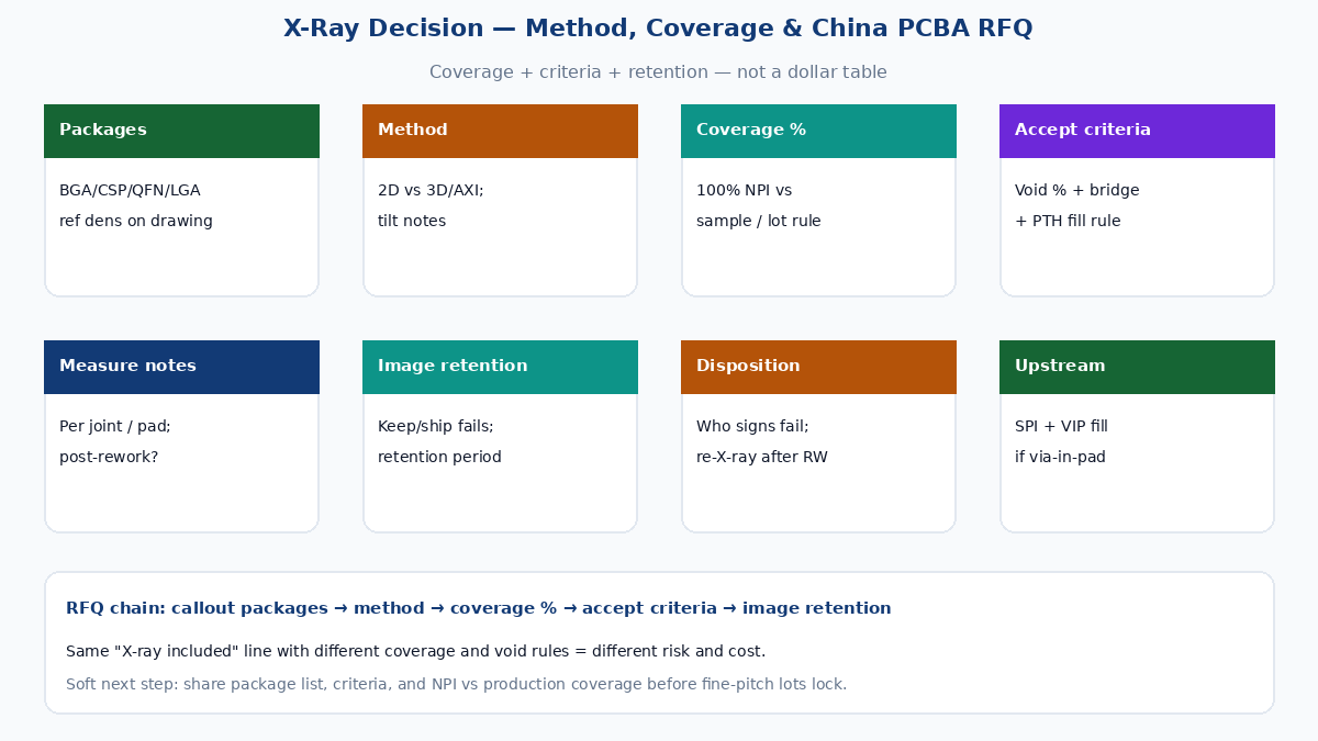
Overseas RFQs that say “X-ray included” inherit house defaults. Normalize these fields so quotes and travelers match:
| RFQ field | Why it matters |
|---|---|
| Packages / ref dens to X-ray | BOM callouts or assembly drawing balloons — not “all SMT” |
| Method | 2D vs 3D/AXI; tilt allowed or not |
| Coverage % | 100% vs sample size / lot rule; NPI vs production split |
| Accept criteria | Void % (area or volume), max single void, bridge = fail, PTH fill rule |
| Measurement notes | Per joint vs per thermal pad; after reflow only vs after rework too |
| Image retention | Keep / ship sample images; retention period; fail-image mandatory |
| Disposition | Who signs fail/rework; whether rework requires re-X-ray |
| Upstream links | SPI required for fine BGA; VIP fill/cap if via-in-pad |
| No silent downgrade | No drop from 100% to sample or from 3D to “photo only” without signed EQ |
Do not paste invented dollar tables or certificate claims into the RFQ cover. Ask for process capability and documented criteria that match the drawing you will freeze. Soft claims that “X-ray always guarantees reliability” are false; X-ray reduces escape of geometric solder defects when criteria and coverage are real.
How this decision sits beside other inspection
Think in layers. SPI catches paste defects before reflow. AOI catches visible post-reflow defects. X-ray catches hidden joints. Flying probe or ICT catches opens/shorts electrically. Functional test catches system behavior. Mandating X-ray does not retire the others; it fills the blind zone under packages and inside selected barrels.
If your program already has a dedicated BGA soldering and void-limit discussion, keep void numbers and reflow ownership there — and keep this page focused on when the X-ray line item is mandatory versus optional. If you are still choosing a broad test mix, treat X-ray as one row in the plan, triggered by package and risk, not as a substitute for a complete inspection strategy.
Common buyer mistakes to avoid. Mandating X-ray with no void or bridge criteria. Asking for 3D on every consumer lot when 2D would catch the fail modes you actually scrap. Sampling only “pretty” boards instead of a random or fixed-interval plan. Leaving image retention blank, then discovering nothing exists for a field return. Quoting three China shops with three different silent defaults because the RFQ never named coverage or method.
Soft next step
Require X-ray / AXI on PCBA when BGA, CSP, QFN, LGA, underfill-hidden joints, or critical PTH fill cannot be judged by AOI or visual methods — and when void, bridge, or fill criteria will actually fail a lot. Prefer 2D for bridges, opens, and many area-void gates; reserve 3D / CT-class work for volume void arguments and complex stacks. Set NPI toward 100% on called-out packages, then sample by proven risk and volume. On China fab RFQs, name coverage %, accept criteria, method (2D vs 3D), and image retention so “X-ray included” means the same traveler in every quote. Share that package with manufacturing engineering before the first fine-pitch BGA lot locks — the right X-ray choice is a quality-plan contract, not a brochure checkbox.