
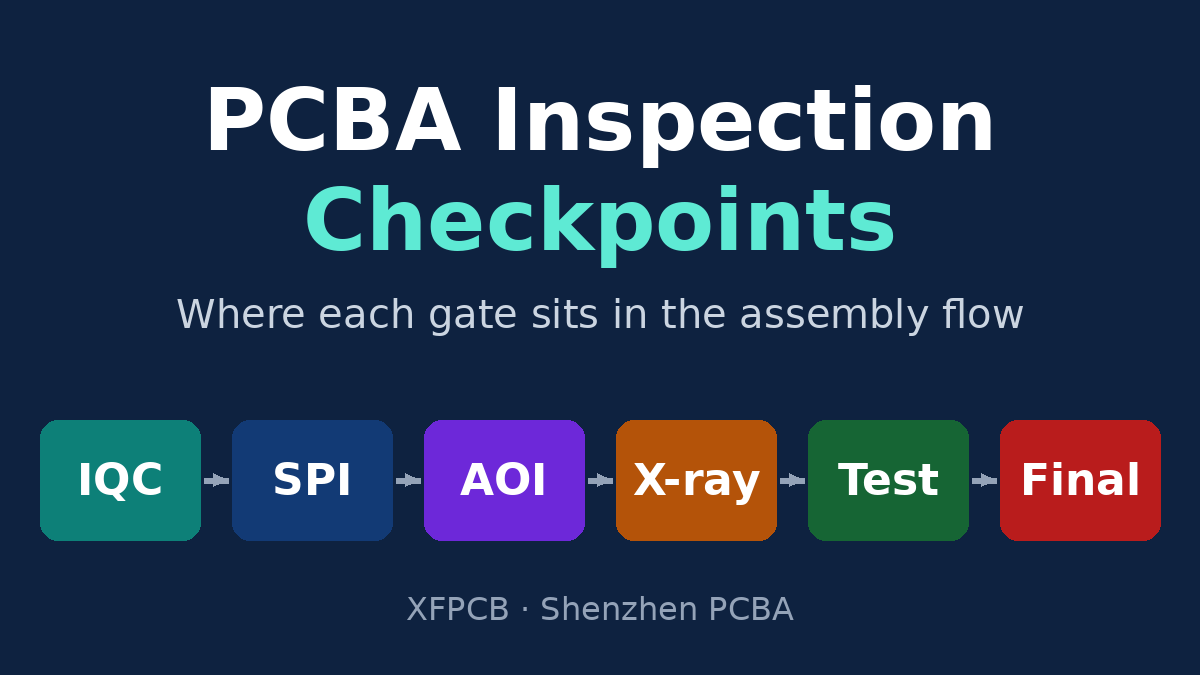
Most buyers first meet PCBA inspection as a list of machines on a capability page: SPI, AOI, X-ray, flying probe. That list tells you what a factory owns. It does not tell you where in your board's route each check happens, what it is supposed to prove at that point, or what happens to a board that fails. Those three things decide whether a defect is caught for the cost of a wipe and reprint, or discovered by your customer.
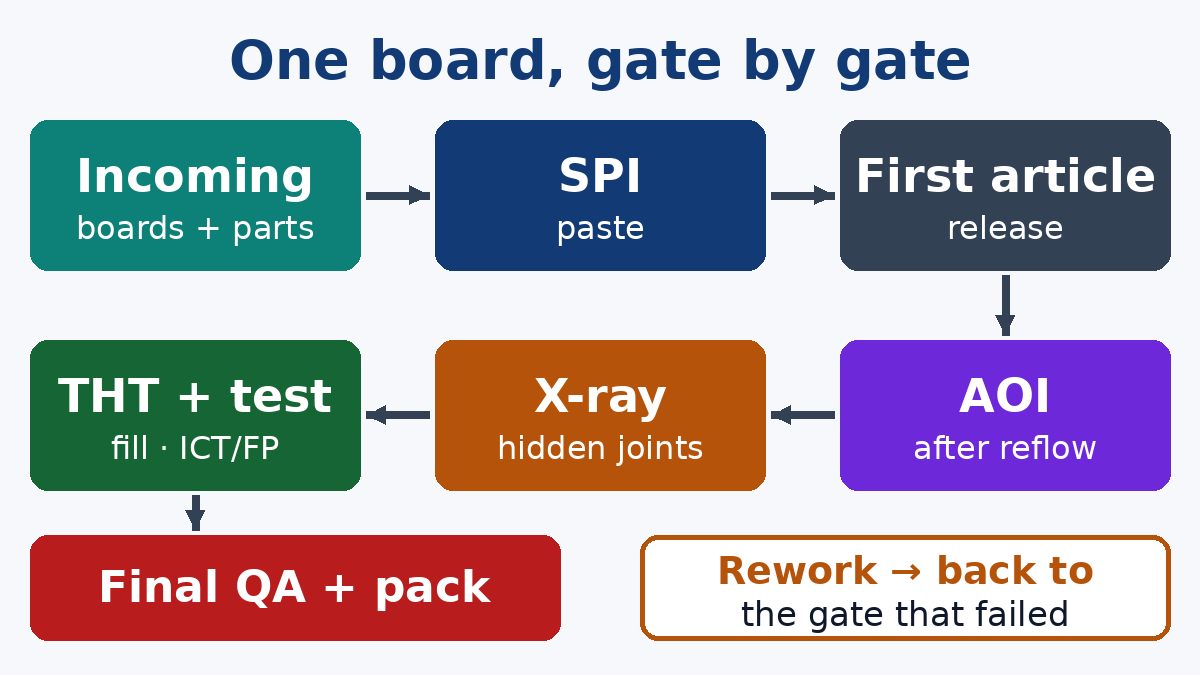
This guide follows one assembly through our Shenzhen line in the order it actually moves, from the dock to the carton, and stops at every checkpoint to ask the same questions: what is this gate for, what can it not see, what record should it leave behind, and what should you, as the buyer, write into the order so the gate is really there. If you want a side-by-side comparison of the inspection technologies themselves, we cover that separately; here the focus is the sequence and the hand-offs between stations.
Why the position of a check matters more than the machine
A defect has a birthplace and a discovery point. Insufficient paste is born at the printer. If nothing looks at the paste, it is discovered after reflow as an open or a weak fillet, and by then the fix involves a soldering iron, extra heat on a component, and a board that is no longer "as built by the process." If the same defect is discovered by final functional test, you may have hundreds of boards to sort.
So the useful question for any inspection step is not "do you have it?" but "how close is it to where the defect is created, and does its result go back to that station?" A good inspection plan puts a gate right after each process that can generate a defect family, and makes each gate talk back to the process before it. A weak plan puts one big optical check at the end and relies on rework.
Stage 0: incoming inspection before kitting
Inspection starts before a single board touches the printer. At incoming (IQC), two different material streams need two different checks.
Bare boards. Check the fab's certificate of conformance and electrical test record against the ordered revision, then look at the boards themselves: surface finish condition, solder mask registration on fine-pitch pads, contamination, and flatness. A bare board that is already bowed will fight the stencil and the reflow conveyor; it is far cheaper to hold it at the dock than to find it as a row of lifted BGA corners. Boards with moisture-sensitive laminates or long storage may need a bake before assembly, and that decision belongs here, not on the line.
Components. Verify part number, manufacturer, quantity, date code and package against the BOM and approved vendor list, and check moisture-sensitive devices for intact dry-pack, humidity indicator card status and the MSL label. Parts from anything other than an authorized channel deserve extra scrutiny: marking quality, lead condition, and where the risk justifies it, a sample sent for deeper analysis.
What the buyer should ask for: an IQC record per lot that ties board and component lots to your work order. If you consign parts, agree in advance what happens when a reel arrives short, mislabeled or with a saturated humidity card, because the factory should stop and ask, not substitute.
Stage 1: paste printing and SPI
Printing is where a large share of SMT solder defects begin, which is why solder paste inspection sits directly behind the printer. SPI measures each deposit's volume, area, height and offset against the stencil design and flags deposits outside the window set for that product.
What SPI proves is narrow but valuable: that the right amount of paste is in the right place before any part is placed. It cannot tell you the joint will be good after reflow, and it says nothing about components.
The real value is the loop back to the printer. A single bad print gets the board washed and reprinted. A drifting trend on one area of the board points to a clogged aperture, worn squeegee, board support problem or a board that is not flat, and the printer is corrected before more boards pass. Ask whether SPI failures on your product are wash-and-reprint or "operator judgement," and whether SPI data for your lot is retained.
Stage 2: first article, before the lot runs
Once the line is set up, the first assembled board is held and checked against the BOM, the assembly drawing and the placement file: every reference designator, value, polarity and orientation. On a new product or a new revision this is the single cheapest insurance you can buy, because one wrong feeder load repeats on every board after it.
We treat first article as a separate topic with its own checklist. In the context of the flow, what matters is that it is a release gate: the lot does not run until someone signs it, and it is repeated after any change that could alter the result, such as a feeder reload with a new reel lot, a program edit, or an ECO.
Stage 3: pre-reflow AOI (optional, but know why you skip it)
An optical check between placement and reflow looks for missing, shifted, rotated or wrong-polarity parts while they are still sitting in wet paste. Fixing a problem here means lifting a part with tweezers and replacing it. After reflow, the same fix means desoldering.
Not every product needs this gate. It earns its place on boards with expensive components, very dense placements, or large parts that are hard to rework once soldered. For a simple board with generous spacing, post-reflow AOI plus a stable first article is usually enough. The point is to decide deliberately. If a factory quotes pre-reflow AOI, ask what it is for on your board; if it does not, ask how placement errors on your most expensive part would be caught.
Stage 4: post-reflow AOI, the main optical gate
After the oven, AOI checks what is visible: part presence, polarity, offset, tombstoning, bridges, insufficient or excess solder on visible fillets, lifted leads. For most SMT boards this is the main in-line quality gate.
Two things decide whether this gate protects you:
- How the program was tuned. An AOI library tuned on a golden board from your first article, with your solder mask colour and finish, behaves very differently from a generic library. Loose tolerances pass real defects; tight tolerances flood the review station with false calls, and operators start waving boards through.
- What happens at the review station. Every AOI call is looked at by an operator who decides "real defect" or "false call." That decision is where a good gate becomes a weak one. Ask who reviews, what reference they use (IPC-A-610 at your class, with visual aids for your board), and whether confirmed defects are logged by location so repeat problems show up.
AOI cannot see under a BGA, a QFN's thermal pad, or any joint hidden by a component body or shield can. It also cannot tell you the circuit works.
Stage 5: X-ray on hidden joints
For area-array and bottom-terminated packages, X-ray inspection is how the joint is inspected at all. The practical buyer questions are about scope: which reference designators, 100% or sample, and what criteria. Voiding criteria for BGAs are commonly discussed with reference to IPC-7095 and your product class under IPC-A-610; state which one you expect rather than leaving it to the operator. If a shield can is soldered over parts, agree whether X-ray happens before the can goes on, because afterwards the view is much worse. We cover the "when is X-ray necessary" decision in its own guide; in the flow, X-ray is a targeted station, not a pass for every board.
Stage 6: the second side, and the through-hole pass
Double-sided boards run the SMT sequence twice. Parts on the first side go through a second reflow upside down, so heavy parts on side one may need glue or a profile check, and the second-side AOI should include a look at side-one parts that could have moved. Buyers sometimes assume one AOI pass covers both sides; ask.
Through-hole assembly follows SMT, with parts soldered by wave, selective solder or hand. This stage has its own defect families: insufficient barrel fill, solder bridges between closely spaced leads, solder balls, flux residue, and lifted connectors. Inspection here is usually a combination of AOI where the machine can see the joint side and trained visual inspection against IPC-A-610 criteria for through-hole joints, including vertical fill requirements for your class. If press-fit connectors are used, the check is insertion force and seating, not solder.
Stage 7: rework and re-inspection, the loop that gets forgotten
Every factory reworks. The risk is not rework itself but what happens after it. A reworked joint should go back through the gate that would have caught the original defect: a reworked BGA goes back to X-ray, a reworked fine-pitch IC back to AOI or magnified visual inspection, a reworked board back through electrical test if the rework came after test.
Rework should follow controlled methods (IPC-7711/7721 is the usual reference), be done by qualified operators, and leave a record: which board, which location, what was done, who did it, and which re-inspection it passed. Two things buyers can reasonably require: a limit on how many times a location or component may be reworked, and visibility of rework counts by board serial or lot. If a factory cannot tell you how many boards in your lot were reworked, the rework loop is not controlled.
Stage 8: electrical test and function
Inspection answers "does it look right?" Test answers "is it connected and does it work?" After soldering, the board goes to in-circuit test or flying probe testing for opens, shorts and component values where there is access, then to functional test if you have supplied a fixture, firmware and a test procedure.
For the inspection plan, the key is the hand-off: a board that fails test should be diagnosed, reworked, and then re-inspected and re-tested, not just re-tested until it passes. Also agree what test coverage your design actually allows. Missing test points mean lower electrical coverage, and that makes the optical and X-ray gates carry more of the load.
Stage 9: cleaning, coating, final QA and packing
The last stretch is easy to under-specify. If boards are cleaned, ionic cleanliness may need checking against the method you agree. If conformal coating is applied, inspect coverage (UV-tracer coatings make this practical), keep-out areas such as connectors and test points, and bubbles or bridging. Depaneling can crack ceramic capacitors near the break line, so final visual inspection should look at parts near the edges.
Final QA then samples the finished lot against IPC-A-610 at your class, checks labels, serials and packaging, and confirms moisture and ESD protection for shipment. This is an audit of the process output, not a substitute for the gates before it.
Writing the stage plan into your order
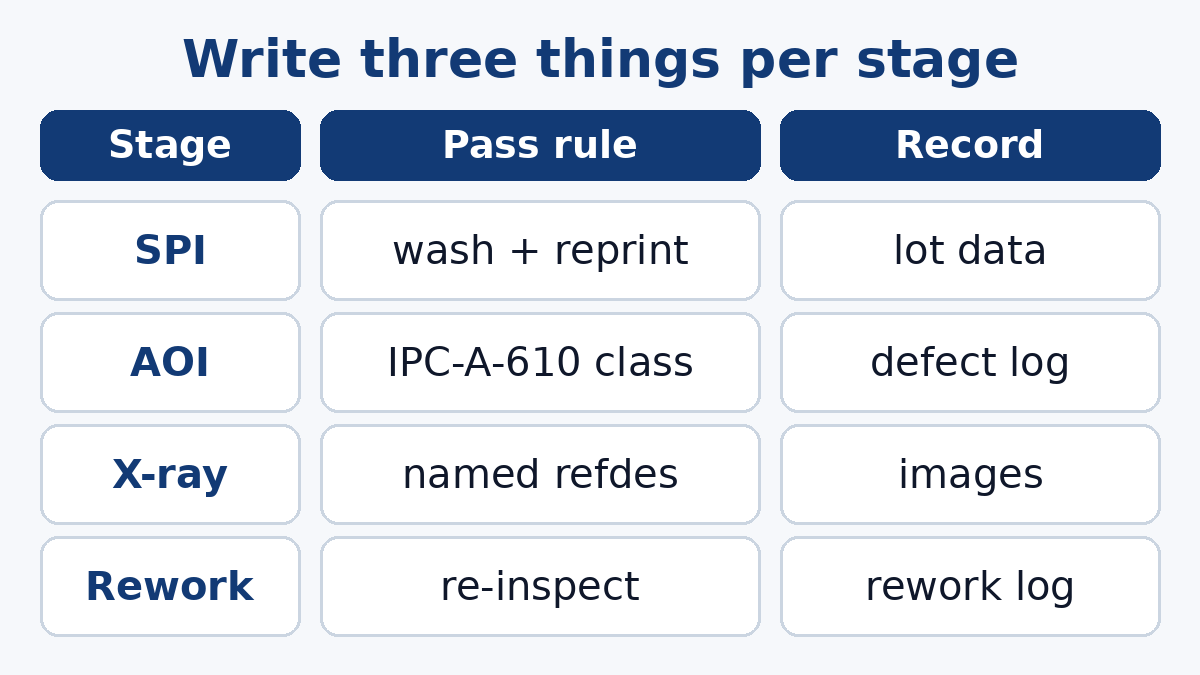
A short inspection clause, stage by stage, removes most of the ambiguity from a PCBA quote. It does not need to be long. For each stage, write three things: whether it applies, the pass rule, and the record you want.
- Incoming: IQC per lot, MSL check for dry-pack parts, bare-board flatness and finish check; stop and ask on any shortage or mismatch, no substitution without written approval.
- SPI: 100% on SMT sides; failed prints washed and reprinted; data kept for the lot.
- First article: full check against BOM and drawing before the lot; repeat after reel change on critical parts, program edit or ECO; report sent to you before shipment on new revisions.
- AOI: post-reflow on every SMT side; pre-reflow only where agreed; workmanship criteria IPC-A-610 Class 2 or 3 as stated on the drawing.
- X-ray: listed reference designators, sample size or 100%, and void criteria.
- Through-hole: fill and bridge criteria per IPC-A-610 at your class.
- Rework: controlled methods, maximum rework cycles per location, re-inspection at the original gate, rework log available by lot.
- Test: flying probe or ICT, plus functional test where you supply fixture and procedure; failed boards reworked, re-inspected and re-tested.
- Final: sampling plan, coating inspection if coated, packaging with moisture and ESD protection.
This is the level of detail at which two quotes become comparable. It is also what lets a factory price honestly, because X-ray on three BGAs at 100% is a different cost from X-ray on a sample.
What a well-run flow looks like from the buyer's side
When the stage plan is working, you notice a few things. Questions arrive before the build, not after: a missing polarity mark, an unclear X-ray scope, a part that needs baking. First-article reports arrive before the lot ships. When something does go wrong, the factory can tell you which gate caught it, which gate should have caught it earlier, and what was changed at the station where the defect was born.
That is the practical difference between a plant that owns inspection equipment and one that runs an inspection plan. If you are preparing a new PCB assembly build and want to walk through which checkpoints your board genuinely needs, send us the files and your class requirement, and our engineers will come back with a stage-by-stage plan along with the quote.