

"Telecom PCB" sounds like one product category. On the factory floor it is at least four. The board inside a radio unit on a tower, the switching card in a central-office chassis, the router in a customer's cabinet and the power shelf that feeds them all share an industry, but they stress a PCB in completely different ways. A buyer who writes one generic "telecom grade" requirement for all of them tends to overpay on some boards and under-specify others.
This guide breaks telecom and network equipment into the board types we see most often in our Shenzhen factory and, for each, describes what the fabrication and assembly process actually has to control and what should be on your drawing. It is written for hardware engineers and buyers sourcing these boards, not as a market overview.
Why telecom boards are different, in general
A few things apply across most telecom equipment:
- Long service lives. Network equipment is expected to run continuously for many years, often in places where replacement is expensive: tower tops, street cabinets, remote sites. That shifts attention to long-term failure mechanisms such as conductive anodic filament growth, via fatigue under thermal cycling, and corrosion.
- Operator and industry requirements. Many operators require equipment to meet NEBS or similar requirements, with Telcordia GR-63 (physical protection) and GR-1089 (electromagnetic compatibility and electrical safety) at the equipment level, and GR-78 covering physical design and manufacture. There is also a telecom addendum to IPC-A-610 for assembly workmanship. These apply to the equipment maker, but they flow down into board requirements, and your PCB supplier needs to know which ones your customer expects.
- Signal performance. Whether it is RF at the antenna or high-speed serial links on a line card, much of the board's value lies in how cleanly it moves signals, which makes material, copper and dimensional control more important than on typical industrial boards.
With that common background, the details diverge quickly.
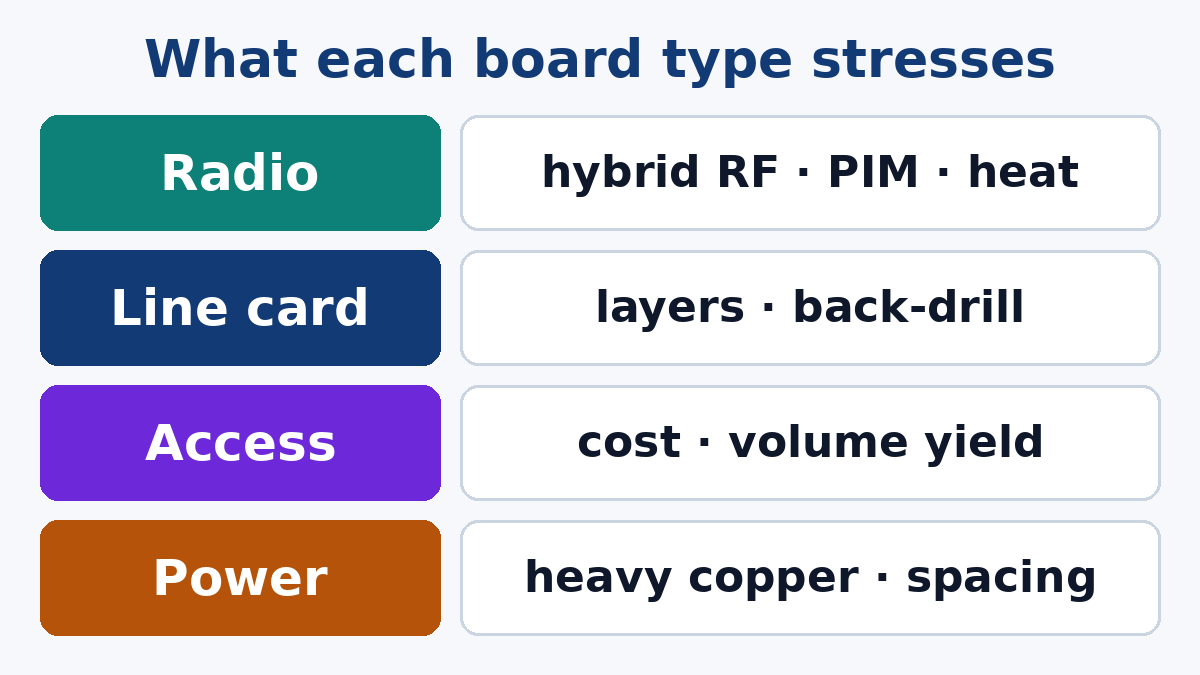
Radio and antenna boards
Radio units, active antenna panels, small cells and microwave backhaul radios carry RF signals at the board level: power amplifiers, filters, feed networks and antenna elements.
Materials. RF sections usually need low-loss, tightly controlled dielectric materials, while control and digital sections work on FR-4. That leads to hybrid stackups, where an RF laminate is bonded to FR-4 in one board. Hybrids save cost but bring their own manufacturing issues: different expansion rates, different drilling and hole-preparation requirements, and bonding films that must be compatible with both. Specify the RF material by name or by required properties and state whether equivalents are acceptable. This is typical High Frequency PCB territory, and it needs a fab that handles those materials routinely, not occasionally.
Passive intermodulation. On antenna feed networks and some filter boards, passive intermodulation (PIM) matters: weak mixing products generated by non-linear materials and junctions, which can fall into receive bands. Surface finish choice is part of it: nickel-containing finishes are generally avoided on PIM-sensitive RF paths, and immersion silver or other nickel-free finishes are often chosen instead. Copper foil roughness, etching quality and clean, well-controlled conductor edges also matter. If PIM is a requirement, say so explicitly and agree how it will be tested (IEC 62037 is the usual reference for PIM measurement), because a board-level PIM test is not something a fab does by default.
Dimensional control. Line widths and dielectric thickness directly set impedance and filter response. Ask for impedance or electrical test on coupons, and understand the fab's etch tolerance on critical RF features.
Thermal paths. Power amplifier stages need heat removed. Common approaches include dense thermal via arrays, copper coins embedded in the board, or bonding to a metal carrier. Each has its own fabrication route and should be designed with the fab involved.
Outdoor exposure. Many radio units live outdoors in sealed enclosures that still see condensation, temperature swings and sometimes corrosive air. Conformal coating is common; where RF performance is affected by coating, its type and keep-out areas must be decided with the RF designer.
Baseband, switching and line cards
Inside the rack, baseband units, switches, routers and optical transport equipment rely on high-speed digital boards: many layers, dense BGAs, high-speed serial links, and often a backplane or midplane connecting cards.
Layer count and thickness. These are often high-layer-count boards with thick overall builds. High Layer Count PCB fabrication brings registration, aspect ratio and plating-uniformity challenges; the fab's ability to hold layer-to-layer registration across a thick stack is often the deciding capability.
Low-loss materials and copper. At high data rates, dielectric loss and conductor loss both matter. Material choice is only half of it; copper foil roughness contributes significantly to loss at high frequencies, so specify foil profile as well as laminate.
Back-drilling. Unused portions of plated vias act as stubs that degrade high-speed signals. Back-drilling removes them from the opposite side after plating. It requires depth control and clear data: which vias, from which side, and to which layer the drill must not reach. Put back-drill layers and depth rules in your data rather than a note.
Press-fit connectors. Backplanes and many line cards use press-fit connectors instead of soldered ones. That puts tight requirements on finished hole size, which depends on plating thickness and the surface finish in the hole. Specify finished hole tolerances per the connector maker's requirements and agree the finish, because some finishes behave better with press-fit than others.
Warpage and flatness. Large, thick boards with many BGAs are sensitive to flatness during assembly. Symmetrical stackups and controlled copper balance matter as much here as on thinner boards.
Reliability testing. Long-life, high-density boards are candidates for CAF-resistant materials and for reliability coupons: interconnect stress testing or thermal cycling of via structures, depending on what your customer requires.
Access and customer premises equipment
Home and enterprise routers, gateways, optical network terminals and similar equipment are high-volume and cost-sensitive.
These boards are usually standard FR-4 multilayers with a mix of RF (Wi-Fi, cellular modules) and digital. The priorities here are cost, consistent yield at volume, and a clean assembly process: fine-pitch SMT, shield cans, and RF matching that does not drift between lots. Specifying a slightly more expensive material or finish than needed repeats across every unit, so it is worth matching the requirement to the actual application rather than applying a generic "telecom" spec. For the Wi-Fi and cellular sections, controlled impedance on antenna feeds and consistent RF matching between lots are what matter most.
Power boards
Telecom sites run on DC power, traditionally a nominal -48 V bus, with rectifiers, battery systems and DC-DC conversion inside equipment.
These boards carry high current and dissipate heat. Thick copper layers, wide conductors, thermal via fields and careful spacing for voltage are the usual features. Heavy Copper PCB construction brings its own manufacturing constraints: etching thick copper limits how fine the features on those layers can be, and lamination must fill the gaps between thick conductors without voids. Spacing and creepage need to be designed for the voltages involved and any safety standard the equipment must meet.
What to write on the drawing
Across all four types, a few items make the difference between a quote that matches your intent and one that does not:
- Performance class under IPC-6012 (usually Class 2 or 3), and any customer flow-downs such as GR-78 or specific reliability tests.
- Materials by IPC-4101 slash sheet or specific product, including RF materials and whether substitutes are allowed, plus copper foil type and profile for high-speed or RF layers.
- Impedance and RF features with tolerances and how they will be verified.
- Surface finish, with PIM or press-fit considerations noted.
- Back-drill and via structures in the data, with depth rules.
- Hole tolerances for press-fit.
- Reliability requirements: CAF-resistant material, coupons for interconnect or thermal cycling tests, cross-sections.
- Assembly class under IPC-A-610 and any telecom addendum requirements, conformal coating specification and keep-outs.
Matching the supplier to the board type
A single supplier does not have to build all four types, and it is worth being honest about fit. A high-volume CPE board and a thick, back-drilled line card need different strengths. When comparing suppliers, ask about the specific capability your board type depends on: hybrid lamination for radio boards, registration and back-drilling for line cards, thick copper for power, and volume consistency for access equipment.
We build boards for Communication Equipment across several of these categories. If you are sourcing one, send us the stackup and drawing, tell us which equipment type and which operator requirements apply, and we will tell you plainly where our process fits and where it would be at its limit.