

A warped board is rarely a mystery about physics. Everyone who has worked with PCBs knows the usual suspects: an unbalanced stackup, uneven copper, moisture, heat. The harder question, and the one that decides who pays and what changes, is where the board became warped. Was it already bowed when it left the fab? Did it go flat into the reflow oven and come out curved? Or was it flat at room temperature the whole time, but moved enough at peak reflow temperature to open a row of BGA joints, then relaxed back so that nothing looks wrong on the bench?
Those three situations have different causes, different owners and different fixes. Treating them as one problem called "warpage" is how buyers end up with a fab tightening its flatness for no benefit while the real cause, a reflow fixture or a package mismatch, keeps producing failures.
This guide is written from the factory floor in Shenzhen, where we build both the bare boards and the assemblies, so we see warpage from both sides. It walks through how to locate the stage that caused it, what evidence to collect, and what each party can realistically change. For the general design rules and limits, our existing warpage guide covers stackup balance, copper distribution and typical bow and twist limits; here the focus is diagnosis.
First, agree on what was measured
Arguments about warpage often turn out to be arguments about measurement.
Bow and twist at room temperature. This is what most drawings and most incoming inspections mean. Bow is a cylindrical or spherical curvature with all four corners in one plane; twist is a deformation where one corner lifts out of the plane of the other three. IPC-TM-650 method 2.4.22 describes how to measure both and express them as a percentage. IPC-6012 sets a default limit for boards with surface-mount parts (0.75%) and a looser one for other boards, unless the drawing says otherwise. If your drawing says nothing, those defaults are what the fab builds to.
Warpage at temperature. A board can pass room-temperature bow and twist and still move significantly during reflow. That movement is measured differently, typically with shadow moiré or similar optical methods on a heated sample, and the relevant guidance is IPC-9641 for boards and JEDEC JESD22-B112 for component packages. Very few incoming inspections include this, which is why "the boards were in spec" and "the BGAs are opening" can both be true.
Panel versus single board. Flatness of a full production panel, an assembly array, and a depaneled single board can be very different. A long, thin array with V-score lines may sag in the oven even if each board is individually flat.
Before anyone assigns blame, write down which of these was measured, how, on how many samples, and at what point in the process.
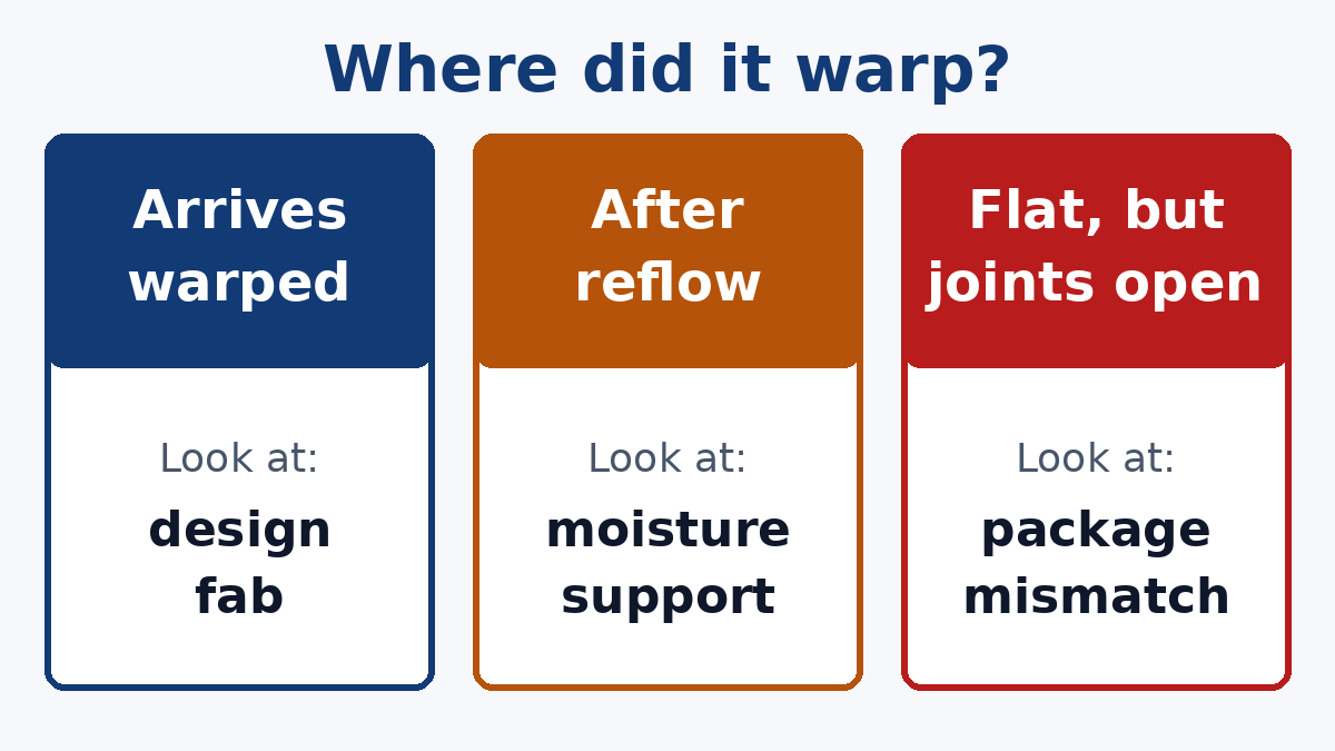
Stage 1: the boards arrive warped
If bare boards fail flatness on arrival, before any assembly heat, the cause lives in design or fabrication. Useful questions:
- Is the warp consistent in direction across the lot? A consistent bow toward the same side usually points to an asymmetry built into the stackup or copper distribution: heavier copper or more copper area on one side of the centerline, uneven dielectric thicknesses, or a hybrid stack of materials with different expansion. Random directions point more toward handling, storage or process variation.
- Does it follow the board or the panel position? Boards from the edge of the production panel behaving differently from those in the middle suggests a lamination or panel-balance issue at the fab.
- Is the design itself asymmetric? Look at the stackup: are cores and prepregs mirrored about the center? Are copper weights mirrored? Is there a solid plane on one side of the center and sparse routing on the mirror layer? A layer pair with very different copper coverage will pull the board toward one side every time it is heated and cooled, and no fab process can fully cancel that.
- Thin board, large outline? Thin boards with long spans have little stiffness. The same asymmetry that is harmless at 1.6 mm can be a problem at 0.8 mm.
At this stage the fab can help in ways the design cannot: balancing copper with thieving in non-functional areas (with your approval, and away from controlled-impedance routing), orienting glass cloth consistently, controlling lamination cool-down, choosing panel layouts that support the board, and, in some cases, a stress-relief bake under weight before shipment. What the fab should not do is flatten boards and ship them without telling you; flattening can relax again during reflow.
If the design is the root cause, expect the fab to report it and propose options rather than simply reject the lot. A stackup change is your decision.
Stage 2: flat in, warped out of reflow
When boards pass incoming flatness and are clearly bowed after reflow, attention moves to the assembly process and to how the design behaves under heat.
Moisture. Laminate absorbs moisture during storage. Heated quickly in reflow, that moisture expands and can distort the board or, in the worst case, cause delamination. Check how long boards were stored, in what packaging, and whether they were baked. Baking is a legitimate countermeasure, but it has costs of its own: over-baking can degrade solderability of some finishes, so the bake conditions should be agreed rather than improvised.
Support in the oven. Boards rest on conveyor rails at the edges. A thin board, or an array with heavy components in the middle, sags at peak temperature when the resin is softest, and the sag partly freezes in as it cools. Center board support, reflow carriers or pallets, and changing the array orientation are assembly-side fixes.
Heavy local mass. Large copper areas, heatsinks, shield cans and big connectors heat and cool at different rates from the rest of the board. A double-sided assembly with dense parts on one side also carries asymmetric mass through the second reflow.
Profile. Ramp rates and cooling rates that are much harsher than the board needs add thermal stress. The profile has to satisfy the solder paste and the most sensitive component first, but within that window there is usually room to be gentler on a warp-prone board.
Material Tg relative to the profile. A standard-Tg laminate spends much of a lead-free reflow profile above its glass transition, where it is far less stiff. Choosing a High Tg PCB material can help a board resist deformation at peak, but it does not fix an asymmetric stackup; it just gives the asymmetry less room to act.
To separate these, run a small controlled test: bake a few boards and reflow them with center support, reflow a few unbaked boards without support, and measure each group before and after. It is quicker than debating.
Stage 3: flat before and after, but joints failed
The most expensive version is the one no one sees. Board and package both move during reflow, and if they move differently at the moment solder melts and solidifies, joints can fail without any visible warpage afterward. On area-array packages this shows up as head-in-pillow defects, where the ball and paste never fully coalesce, or non-wet opens at the corners of a large BGA, or bridging where the gap closes. Often the pattern is geometric: failures cluster at corners or along one edge of the package.
This is a mismatch problem, not a board-flatness problem. The package has its own warpage curve over temperature, which component makers often publish or can provide, and the board area under the package has its own. When the two curve in opposite directions at the critical temperature, the gap at the corners opens.
Evidence that points here: X-ray images showing head-in-pillow or corner opens on specific packages, failures that appear after thermal cycling or on the second reflow, and a board that measures within room-temperature limits. Countermeasures span both sides: local copper balance under the package, stackup changes, stencil adjustments to put more paste at corners, profile changes to reduce time at high temperature, and sometimes a different package supplier. For BGA PCB designs with large packages, it is worth asking for package warpage data during component selection rather than after the first failures.
After assembly: in-service and depaneling
Warpage can also appear after the board leaves the line. Depaneling by hand or with poor tooling bends the board and can crack ceramic capacitors near the break line. Enclosures that clamp a board at points that are not coplanar will force it into a curve every time it is installed. Conformal coating and potting shrink as they cure and, on thin boards, can add a small amount of bow. Board edges near heavy connectors take repeated insertion forces. These are mechanical design issues rather than fabrication ones, but they often get reported as "the PCB is warped."
The evidence to collect before you call the supplier
A warpage complaint with data gets resolved in days; one without data can take weeks. Collect:
- Bow and twist measurements on a sample of bare boards from the same lot, with the method stated.
- The same measurement on assembled boards, and if possible on bare boards that went through reflow without parts.
- Photos showing the direction of the warp relative to the top side and to the panel position.
- Storage and bake history: dates, packaging, humidity indicator status, bake conditions.
- Reflow details: profile, support method, array orientation.
- For joint failures: X-ray or cross-section images and the location of failed joints on the package.
- The stackup and copper coverage per layer, which your fab can usually provide from CAM.
With those in hand, the stage is usually obvious, and the conversation moves from "whose fault" to "what do we change."
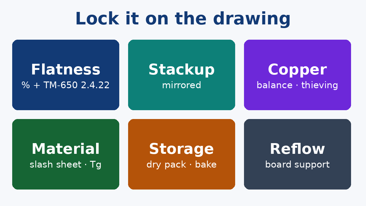
What to put on the drawing and the order
Prevention is still cheaper than diagnosis. A few lines on the fab drawing and assembly order go a long way:
- Flatness requirement and method: the bow and twist limit you actually need, measured per IPC-TM-650 2.4.22, and whether it applies to the single board or the delivered array.
- Stackup symmetry: a stackup that is mirrored about the center, or explicit acceptance of an asymmetric one with a warpage expectation agreed in advance.
- Copper balance: permission, or not, for the fab to add thieving in non-functional areas, and keep-outs for impedance-controlled nets.
- Material: IPC-4101 slash sheet and Tg appropriate for your reflow profile, rather than a generic "FR-4."
- Packaging and storage: vacuum packing with desiccant and humidity indicator, and a bake rule before assembly if storage exceeds an agreed time.
- Assembly support: reflow support or carriers for thin or large boards, and array design that gives the assembler somewhere to support the board.
- Critical packages: for large BGAs, a request for package warpage data and X-ray on first article.
If you are seeing warpage on a current build and are not sure which stage it comes from, send us the stackup, a few measurements and photos. Because we run both fabrication and SMT, we can usually tell quickly whether the answer is in the laminate, the oven or the design, and propose the smallest change that fixes it.