
"Motherboard" makes most people think of the large board inside a desktop PC. For the hardware companies we build for, it usually means something smaller and more specific: the main board of their own product. That might be the board inside an industrial controller, a medical display, a kiosk, a gateway or a robot. It carries the processor, the memory and most of the connections to everything else in the device.
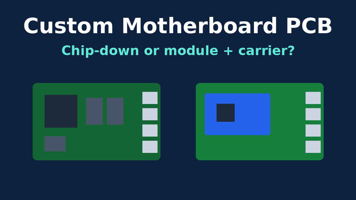
This article covers the terms briefly, then the decision that shapes almost everything about a custom main board: whether to put the processor and memory directly on your own board (often called chip-down design) or to buy them on a ready-made compute module and plug it into a simpler carrier board. The choice changes the PCB technology, the assembly and test work, the sourcing risk and the cost structure, and it's much easier to make deliberately than to undo.
Motherboard, PCB and PCBA: the terms
A PCB is the bare board: glass-epoxy layers, copper traces and planes, vias, pads, solder mask and legend. A PCBA is that board with components soldered on. A motherboard (or main board, or system board) is a particular PCBA: the one at the centre of a system that the processor, memory, storage and peripherals all connect through.
So a motherboard is a PCB-based assembly, but most PCBs aren't motherboards. A power supply board or an LED driver is a PCBA with one job. The motherboard is where the system comes together, and that concentration of fast signals, many power rails and many connectors is what makes it harder to design and build than most boards in a product.
What makes a main board demanding
Whatever the product, a main board tends to combine the same difficult elements in one place:
- A processor in a fine-pitch BGA package. Getting all its connections out from under the package (BGA escape routing) often decides the layer count by itself.
- Fast memory. DDR interfaces need matched lengths, controlled impedance and clean reference planes.
- Many power rails. A modern processor needs several supply voltages, sequenced correctly, with low-impedance delivery to the package.
- High-speed interfaces. USB, PCIe, Ethernet, display links and others, each with impedance and routing rules.
- Lots of connectors. These are mechanical as well as electrical parts, with their own placement, strength and assembly demands.
The chip-down versus module decision is really a decision about how many of these you take on yourself.
Option 1: Chip-down, with everything on your board
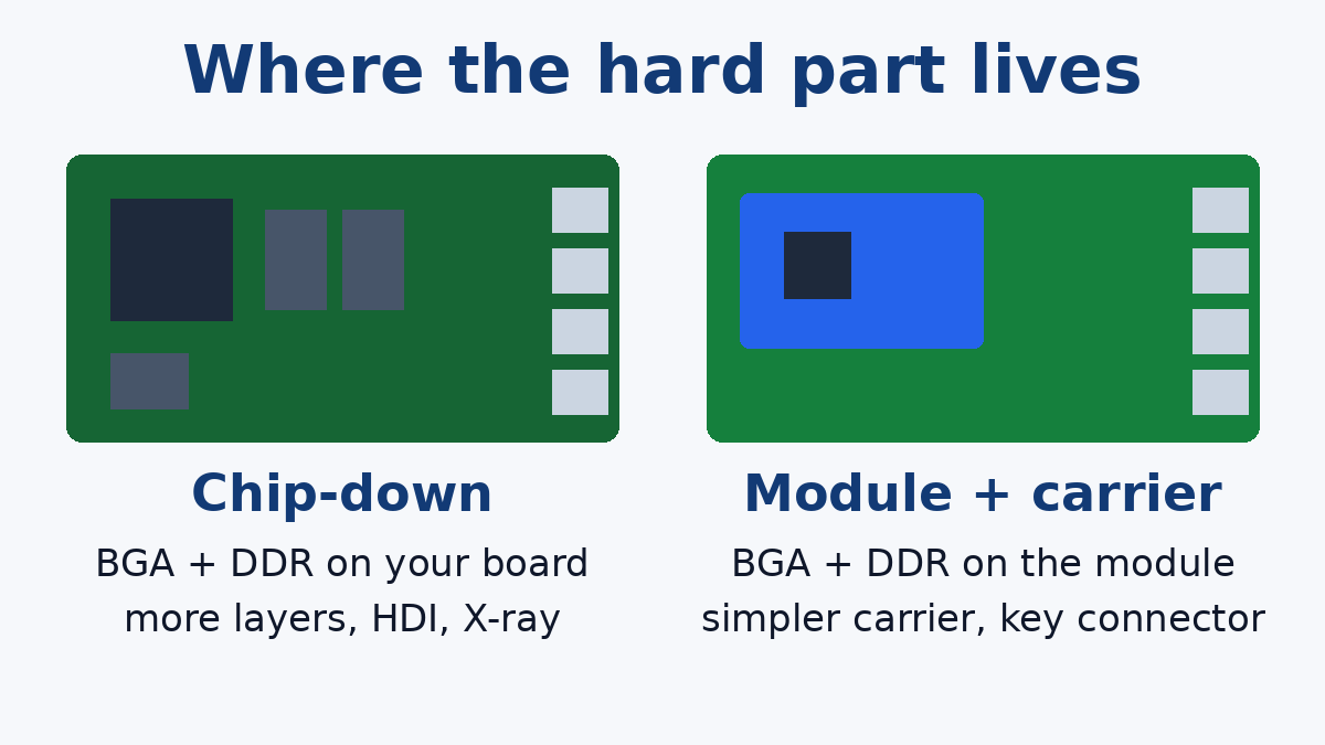
In a chip-down design, the processor, memory, flash, power management and clocks are all placed on your main board.
What it means for the PCB. Fine-pitch processor packages and DDR routing usually push the board to more layers, and very fine BGA pitches often need microvias, which means HDI PCB construction with sequential lamination. The stackup has to be planned with controlled impedance from the start, and the memory routing has to be designed and checked against the processor vendor's layout rules. The board is more expensive to fabricate per square centimetre, and design errors are expensive too, because a respin of a dense multilayer board takes time.
What it means for assembly and test. Large, fine-pitch BGAs can't be inspected visually once they're soldered, so solder joint quality is checked by X-ray, and paste printing, placement and the reflow profile all need to be right for those parts. Bring-up is a real engineering phase: power sequencing, memory training and boot have to work on the first prototypes, or someone has to find out why. Production testing usually needs a way to program the device and exercise its interfaces, and boundary scan through the processor's JTAG port, where available, can test connections that a probe can't reach.
Why choose it. You control the form factor completely. At high volume, the bill of materials can be lower than buying a module, because you're not paying for a second PCB and someone else's assembly and margin. You also control the lifecycle: which parts are used, and when they change.
Option 2: A compute module on a carrier board
A compute module (often called a system-on-module, or SoM) is a small, finished board carrying the processor, memory, flash and power management, already assembled and tested by its maker. Your main board becomes a carrier: it supplies power, routes the module's interfaces out to connectors, and holds the product-specific circuits.
What it means for the PCB. The hardest routing (BGA escape and DDR) lives on the module, so the carrier is usually a simpler multilayer board, often with fewer layers and no microvias. It's not trivial, though. Any high-speed interfaces leaving the module (USB, PCIe, Ethernet, display) still need controlled impedance across the carrier, so the stackup still needs proper planning, just for fewer and shorter critical routes.
What it means for assembly and test. The module connector becomes a key part. Fine-pitch board-to-board connectors need good paste printing, coplanarity and placement. Edge-card style modules need the right socket and mechanical retention. Testing the carrier is simpler because the processor is already proven. A known-good module plugged into each carrier during functional test checks the carrier's own circuits.
Why choose it. Much less design risk and a faster path to working hardware. The processor and memory design, often the riskiest part, is already done and validated. Many modules also come with board support software, which can matter as much as the hardware. The trade-offs are a higher cost per unit at volume, a mechanical envelope set partly by the module, and a dependency on the module maker for supply and lifecycle.
What each choice asks of the factory
| Chip-down main board | Carrier board with module | |
|---|---|---|
| Layer count | Usually higher, set by BGA escape and DDR | Usually lower, set by interfaces and power |
| HDI / microvias | Often needed for fine-pitch BGAs | Usually not needed |
| Controlled impedance | DDR plus all high-speed interfaces | High-speed interfaces leaving the module |
| Critical assembly | Fine-pitch BGAs, X-ray inspection | Module connector or socket |
| Bring-up | Power, memory and boot on your board | Mostly carrier circuits |
| Production test | Programming, boundary scan, interface test | Functional test with a known-good module |
| Supply risk | Processor, memory and power parts | The module and its maker's lifecycle |
Assembly details worth settling early
Whichever route you choose, a few assembly questions are cheaper to answer before layout than after:
- BGA rework. If the processor or memory must be reworkable, keep room around them for a rework nozzle, and avoid tall parts right next to them. Our BGA PCB page lists the checks we make on BGA-heavy boards, such as via-in-pad and solder mask registration.
- X-ray access. Components on the opposite side directly under a BGA make X-ray images harder to read. Where you have a choice, keep the area under large BGAs clear on the other side. X-Ray Inspection is how hidden BGA joints are checked for voids and bridges, and clear images make that check meaningful.
- Connector strength. Large connectors that take repeated mating forces need through-hole posts, mounting screws or a mechanical support, not just surface-mount pads.
- Test access. Plan test points for power rails and key signals, and decide early how firmware will be loaded in production.
Sourcing and lifecycle
A main board's bill of materials is usually where supply risk concentrates. On a chip-down board, the processor, memory and power management IC are often single-source. Memory in particular is worth qualifying with more than one approved part, because memory availability changes faster than most other components. On a module design, the risk shifts to the module: check its maker's long-term availability commitment and what happens when the module is updated.
For a product with a long service life, such as industrial equipment or medical devices, lifecycle often decides the question more than unit cost does. If the module maker's roadmap matches your product's life, a module is a safe choice. If you need to control the parts yourself for many years, chip-down gives you that control at the price of doing the design work.
A common middle path
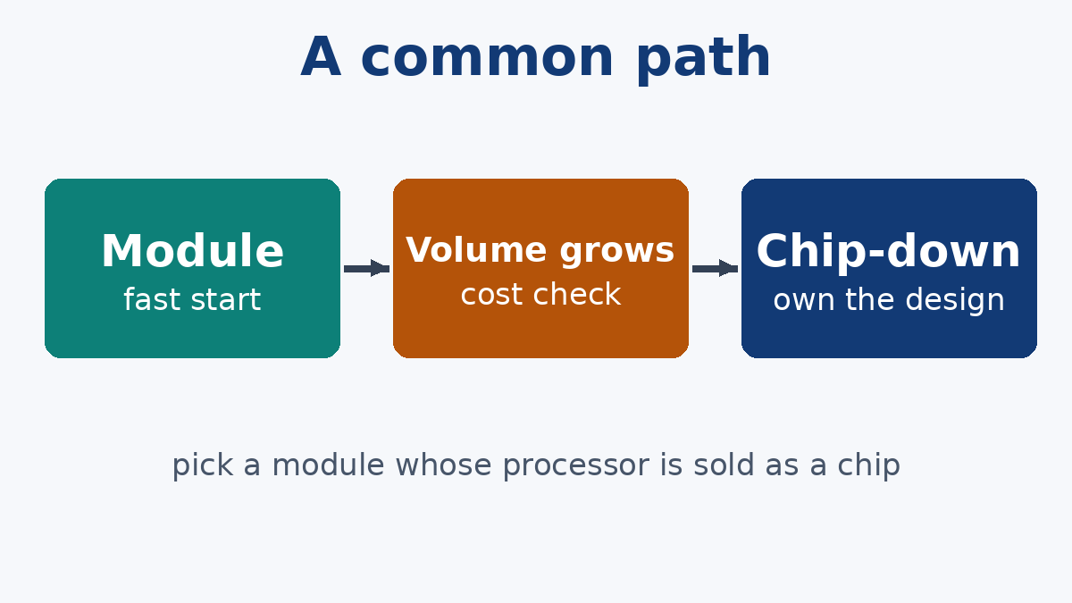
Many products start on a module and move to chip-down later. The module gets working hardware and software into customers' hands quickly. If volumes grow to the point where the module's cost premium outweighs the cost of a chip-down design, the processor section is redesigned onto the main board, often reusing the module maker's reference design as a starting point. If you think that's likely, choose a module whose processor is also available as a chip, and keep the carrier's interfaces aligned with what the chip-down version will provide.
What to send for a quote
- Gerber or ODB++ files, drill files and a fab drawing with the stackup and impedance table.
- The BOM with manufacturer part numbers, flagging single-source and long-lead parts and any approved alternates.
- Which parts are BGAs, their pitch, and any rework or underfill requirements.
- For carrier boards, the module and connector part numbers and the mating height.
- Test expectations: programming, boundary scan, functional test and who provides fixtures and firmware.
- Volumes for prototype, pilot and production, which affect both the build approach and the sourcing plan.
If you're still deciding between chip-down and a module, we can quote both versions of the board side by side, which often makes the decision clearer than any rule of thumb.