
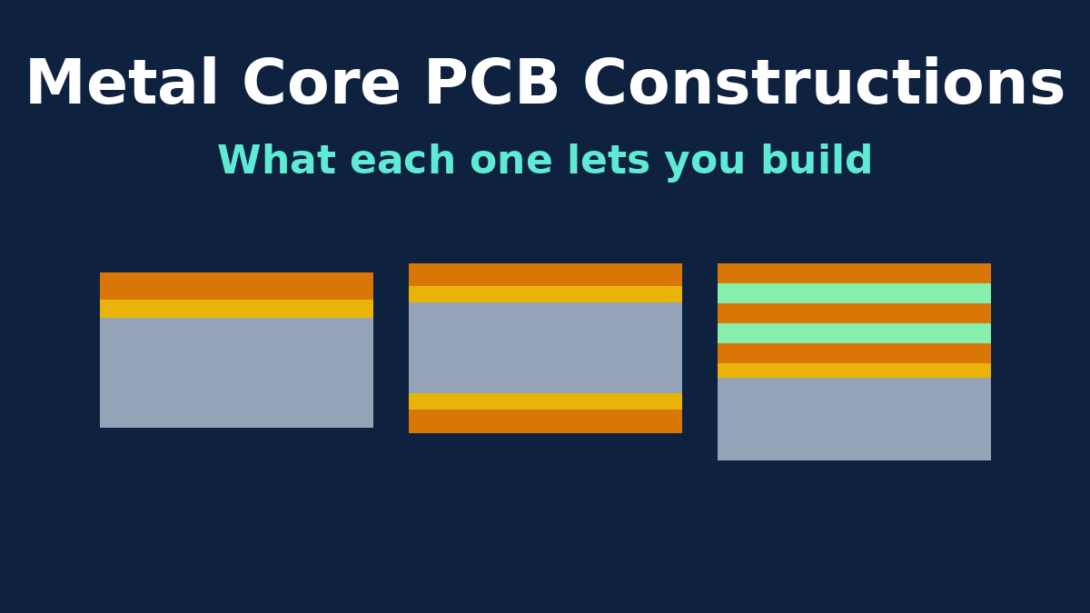
"Metal core PCB" covers a family of very different boards. Some are a single copper layer on aluminium that any LED module maker would recognise. Others have a metal core buried in the middle of a multilayer stack, or a copper base machined so that a component sits directly on the metal. They differ in what you can route, which sides take components, whether through-hole parts are possible, and above all in whether the heat has to cross a dielectric layer on its way to the metal.
This article sorts the common constructions by those questions. Base metal and dielectric grades are a separate decision, covered in our metal core materials article. Here the subject is the arrangement of layers, and what each arrangement lets you do.
Two questions that sort every construction
Before looking at the options, it helps to know which two questions separate them.
How many copper layers do you need, and on which side? A circuit with no crossovers can live on one layer. A circuit that needs a ground plane, crossings or dense routing needs more. Components on both sides, or through-hole parts, rule out the simplest builds.
Does the heat from the hottest part have to cross a dielectric? In most constructions it does, and the dielectric is the weakest step in the thermal path. A few constructions let the hot part's thermal pad touch the metal directly, at the cost of extra machining and an electrical consequence discussed below.
Single-layer: one copper layer on a metal base
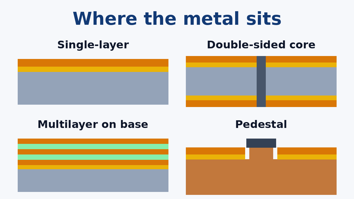
This is the familiar insulated metal substrate: copper circuit, thermal dielectric, metal base. Components go on the copper side only, and they're surface-mount. Through-hole leads would pass through the metal, so they need insulated holes and aren't a natural fit.
It's the simplest and usually the least expensive construction because it's made from a ready-laminated material with a single print-and-etch cycle and no lamination in the factory. It suits LED boards, simple power stages and anything whose circuit has no crossovers.
A practical tip: if a single-layer design needs one or two crossings, a zero-ohm resistor or a jumper part can bridge them. A handful of links often keeps a design on single-layer construction when the alternative would be a much more complex build.
Two copper layers on one side
When a single layer can't route the circuit, the next step keeps both copper layers on the same side of the metal. An imaged two-layer circuit is bonded to the metal base with a thermal dielectric, and vias connect the two copper layers but stop above the base.
Components are still surface-mount on one side. The new thermal consideration is that a part on the top layer now sends its heat through the dielectric between the two copper layers as well as the one bonding them to the base. Vias under hot pads, connecting down to copper on the lower layer, help carry heat past that extra layer. The design rules are those of a two-layer board, with the extra constraint that no plated hole may reach the metal.
Double-sided with the metal core in the middle
Here the metal sits in the centre of the stack, with dielectric and copper on both outer faces. Components can be placed on both sides, and through-hole parts are possible, because plated holes pass through the core.
To make that work without shorting every hole to the core, the core is drilled oversize first and the clearance filled with insulating resin before the final hole is drilled and plated. It's a more involved process, and the registration between the clearance hole and the final hole sets how close plated holes can sit.
The thermal picture changes too. Neither outer face is bare metal, so there's no flat metal back to clamp to a heat sink. The core spreads heat sideways very well, but the heat still has to leave somewhere: through a dielectric to one face, or through the board edges or mounting points where the core is exposed. This construction is often chosen for stiffness and spreading inside an enclosure rather than for direct heat sinking.
Multilayer on a metal base
When the circuit needs real multilayer routing (power and ground planes, many signals, fine-pitch parts), a multilayer board is built and then bonded to a metal base with a thermal dielectric. All the routing freedom of a multilayer board is available above the metal, including blind vias down to the lowest layer, but components remain on the top side.
Heat from a top-side part crosses several layers to reach the base, so arrays of vias under the hot pads, carrying heat down to the bottom copper layer, do most of the work. Those vias have to stop at the bottom copper layer, above the bonding dielectric, never plating into the metal. The build involves at least one extra lamination, a thicker overall board, and stack balance to watch, because the metal and the multilayer expand differently and an unbalanced build can bow.
Pedestal (direct thermal path) on a copper base
This construction removes the dielectric from the main heat path. A copper base is machined so that raised pedestals stand up through openings in the dielectric and circuit layer, finishing level with the surrounding pads. A component's thermal pad is soldered straight onto a pedestal, so its heat goes into solid copper without crossing any dielectric. The other pads (the electrical connections) sit on the normal insulated circuit beside it.
The thermal improvement can be large for a part that dissipates a lot from a small pad. The consequences need to be understood before choosing it:
- The thermal pad is electrically connected to the base. That only works if the component's thermal pad is electrically neutral, or if you accept the base sitting at that pad's potential. Many LED packages have an isolated thermal pad. Many power packages don't, because their tab is the drain or collector. Check the datasheet before planning a pedestal.
- If the base is live, the housing interface must be insulated. A base connected to a circuit node can't simply be bolted to a grounded chassis.
- Pedestal height and position are critical. The pedestal has to finish level with the circuit pads and line up with the package footprint within tolerance, or the solder joint suffers. It's a machining and lamination process with tighter tolerances than a standard build, and it's typically more expensive.
Chip-on-board on metal
In a chip-on-board construction, bare dies (most commonly LED chips) are attached directly to the metal or to a prepared area on it and wire-bonded to the circuit. Like the pedestal, it takes the dielectric out of the heat path for the die. It also moves part of the work from PCB fabrication into die attach and wire bonding, which needs a bondable surface finish and assembly capability that a standard SMT line doesn't have. The same electrical point applies: whatever potential the die backside has, the metal it sits on shares it.
Conventional board bonded to a shaped heat sink
A different approach keeps a normal FR-4 board and bonds or presses it onto a metal plate or a shaped heat sink, sometimes only under the hot area. Routing is unrestricted on the FR-4, and the metal adds local cooling and mechanical strength. The heat still has to get through the FR-4, usually by thermal vias under the hot parts, and the quality of the bond between the board and the metal decides how well it works. Flatness, bond voids and stress at the edge of the metal area are the things to control.
If the heat problem is a single hot package on an otherwise dense multilayer board, an embedded copper coin in a standard multilayer is another option. We cover it in a separate article on embedded copper coin PCBs.
Side by side
| Construction | Copper layers | Component sides | Through-hole | Heat crosses dielectric? | Main fabrication complexity |
|---|---|---|---|---|---|
| Single-layer | 1 | One | Not practical | Yes, once | Lowest |
| Two layers on one side | 2 | One | No | Yes, twice unless vias help | Bonding a circuit to metal |
| Double-sided core | 2 | Both | Yes | Yes | Resin-filled holes in the core |
| Multilayer on base | 3+ | One | No | Yes, via arrays needed | Extra lamination, stack balance |
| Pedestal | Usually 1 | One | No | No, for the pedestal pad | Machined base, tight tolerances |
| Chip-on-board | 1 | One | No | No, for the die | Die attach and wire bonding |
| Bonded heat sink | Any FR-4 | Usually one over metal | On FR-4 areas | Through FR-4 and vias | Bond quality and flatness |
Choosing: start simple and add only what the design forces
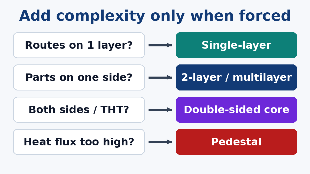
A useful way to choose is to start with single-layer and move up only when something forces it:
- Can the circuit route on one layer, perhaps with a few links? If yes, single-layer.
- If not, are all components on one side? If yes, two layers on one side, or a multilayer on metal if you need planes.
- Do you need components on both sides or through-hole parts? Then the double-sided core, accepting the different thermal path.
- Is one part's heat flux too high for any dielectric, and does it have an isolated thermal pad? Then a pedestal.
It's also worth asking whether the whole circuit has to be on metal at all. A common and often cheaper arrangement is to split the design: the hot parts (LEDs, power devices) on a single-layer metal core board, and the control circuit on an ordinary FR-4 board, joined by a connector or wires. Each board then uses the simplest construction that suits it.
What to tell the factory
Not every factory builds every construction, and the process routes differ a lot, so the quote request should state the construction plainly:
- A sketch or stack table showing which layers sit where relative to the metal.
- Copper layer count, component sides and whether through-hole parts are present.
- For pedestal builds, which pads sit on pedestals and their electrical role.
- The insulation requirement between circuit and base, and whether the base is live.
When a Metal Core PCB request comes to us without a clear construction, our first question is usually which of these arrangements is intended, because the answer changes the process, the design rules and the cost far more than the choice of dielectric does.