
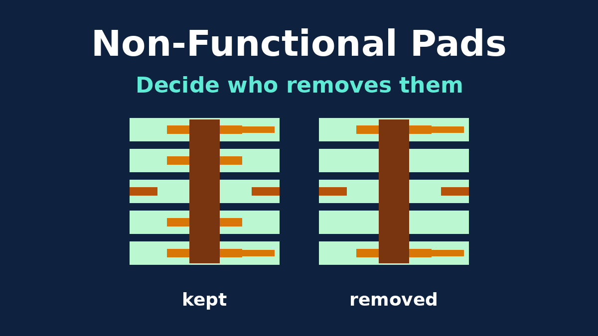
Non-functional pads are the copper rings around a plated hole on layers where nothing connects to it. Most discussion of them is about whether they should stay or go: they take routing space and add capacitance, and in some boards they may help the plated barrel. That debate matters, but on real orders the more common problem is simpler. Nobody has said who decides. The layout tool removes some pads, the factory's CAM team removes others by default, the signal integrity model assumes a third arrangement, and the fab drawing says nothing.
This article looks at non-functional pads from the CAM side: where the decision can be made, how a factory identifies them, which holes deserve an exemption, and the short fab notes that keep the design data, the model and the finished board in agreement.
A quick definition
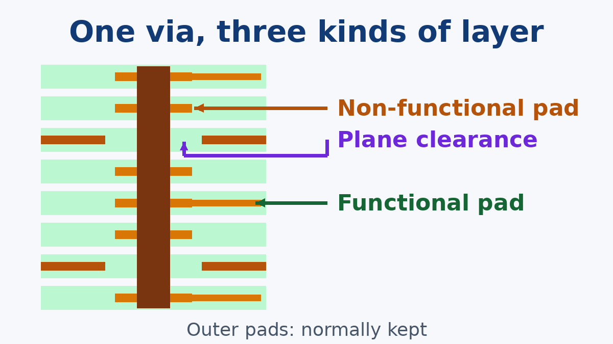
Take a through via on an eight-layer board that connects a trace on layer 1 to a trace on layer 6. On layers 1 and 6 it has functional pads, because copper connects to them. On the other signal layers it may carry an annular ring that connects to nothing. Those are non-functional pads (NFPs). On plane layers it passes through, the via normally sits in a clearance hole in the plane, called an antipad, unless it connects to that plane.
Outer-layer pads are a separate matter. The rings on layers 1 and 8 support plating at the hole entry, solder mask registration and inspection, and they're normally kept even if nothing connects to them. When people talk about removing NFPs, they almost always mean inner layers only.
Three places the decision gets made
In layout. Most design tools can remove unused pads per via or per padstack. The designer then exports data without NFPs, and the factory builds what it receives.
At the factory, in CAM. CAM engineers prepare the production data from your files. Many factories remove inner-layer NFPs as standard practice on rigid boards, mainly because every extra copper ring the drill cuts through adds drill wear and heat, and trade-press surveys of fabricators have found removal to be common, done routinely or with customer approval.
Both, or neither, without anyone saying. This is where the trouble starts. If the designer kept NFPs on purpose (for a thick board, a press-fit connector or a flex layer) and the factory removes them by default, the board isn't what was intended. If the designer modelled a high-speed via without NFPs but the data still contains them and the factory leaves them in, the via has more capacitance than the model.
The fix isn't a particular policy. It's a sentence on the drawing that says which policy applies.
The rule that matters if you remove them in layout
If you remove NFPs in your design tool, route with them in place first and remove them afterwards. IPC-2221's design guidance makes the same point: internal lands shouldn't be removed simply to make room to route between holes.
The reason is that removing a pad doesn't remove the hole. The drilled hole still wanders a little, inner layers still shift slightly during lamination, and drilling, desmear and plating all affect the copper close to the hole wall. A trace squeezed into the space a pad used to occupy can end up too close to the plated barrel. That's a risk of shorts at test and, over time, of conductive anodic filament growth between the hole and the trace. Keeping the drill-to-copper clearance you'd have with pads in place avoids it.
How CAM finds non-functional pads
To remove NFPs, CAM has to know which pads are connected. With Gerber files, the connectivity is derived from the copper itself: a pad touching a trace or plane is functional, an isolated ring is not. That works, but it relies on the copper data being right.
An IPC-D-356 netlist exported from your design gives CAM an independent reference. It's used for electrical test anyway, and comparing it with the connectivity derived from the copper confirms that nothing functional is about to be removed and nothing non-functional is left by mistake. ODB++ and IPC-2581 carry net information within the data. If you send Gerbers, include the netlist. Our Manufacturing Files page lists what to send with an order.
Which holes deserve an exemption
If you allow removal, it's often worth naming the holes where NFPs should stay:
- Component holes, especially press-fit. Through-hole and press-fit connectors put mechanical load on the plated barrel. Many designers keep inner lands on these holes as a matter of course.
- Thick, high-aspect-ratio boards in harsh thermal cycling. Some fabricators report that on thick, high-layer-count boards with few internal connections, inner lands reduce barrel and pad problems through repeated heating. The evidence is mixed and depends on the construction, so it's a decision to discuss with the factory rather than a rule. If the board is in this category, ask.
- Flex and rigid-flex layers. Copper adhesion and the behaviour of plated holes in flexible materials differ from FR-4. Removing every inner land from holes through flex layers deserves a specific review.
And the holes where removal is usually wanted:
- High-speed signal vias. NFPs add capacitance to a via. FPGA and transceiver vendors' layout guidance commonly recommends removing them on multi-gigabit vias.
- Dense fanout areas. Under fine-pitch BGA PCB designs, removing inner NFPs opens routing channels and helps keep the drill-to-copper margins healthy.
- Ordinary signal and stitching vias on rigid boards, where removal mainly helps drilling.
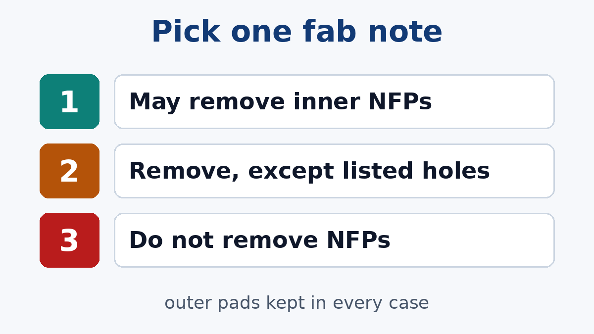
Three fab notes that cover most boards
Pick one and put it on the drawing:
- "Non-functional pads on inner layers may be removed. Outer-layer pads shall be retained." For most rigid boards. The factory follows its normal practice.
- "Non-functional pads on inner layers may be removed, except on the holes listed in [table or drill tool numbers], where all lands shall be retained." For boards with press-fit connectors, flex layers or other exceptions.
- "Non-functional pads shall not be removed. Data is supplied with pads as intended." When the design depends on them, or when NFPs were already removed in layout exactly as wanted and nothing further should change.
If your signal integrity model depends on the via structure, state it: for example, "high-speed vias modelled without non-functional pads; data supplied accordingly." That tells CAM the absence of pads is deliberate.
How to check what you'll get
- Read the engineering questions. If a factory plans to change pads and your notes don't cover it, it should ask before production. Answer with reference to the note, so the next order follows the same rule.
- Review the working data if offered. Some orders include CAM output for approval. A quick look at an inner layer in a dense via field shows whether NFPs are present.
- Section a sample if it's critical. A microsection through a via shows the lands on each layer, which settles the question on high-reliability programmes.
A short checklist
- Decide the NFP policy before layout is released, not after a CAM question arrives.
- If removing in layout, route with pads in place, then remove.
- Send an IPC-D-356 netlist with Gerber data.
- Use one of the three notes, with an exemption list if needed.
- Keep outer-layer pads unless the factory agrees otherwise.
It's a small note on a drawing, but it decides how every via in the board is built, and it's much easier to write once than to explain after a lot is made.