
"Parts of a PCB" can mean two things. One is the components soldered onto the board: resistors, capacitors, ICs and connectors. The other is the board itself, the layered structure that holds those components and connects them. This guide is about the second meaning: the parts of the bare printed circuit board, from the glass-reinforced core to the white lettering on top.
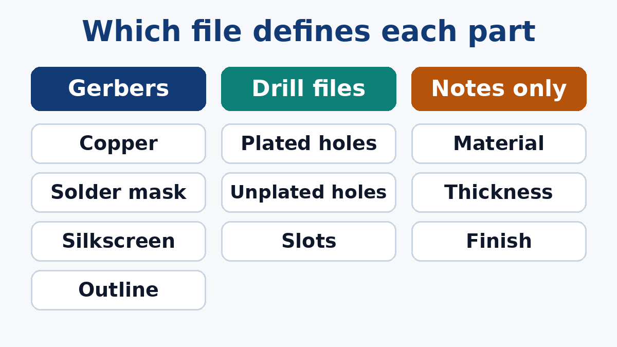
For each part, we'll cover what it is, what it does, and how it's described to a factory. That last point is where most beginners get caught out. Some parts are drawn in the Gerber files, some come from the drill file, and some exist only as a line of text on a fabrication drawing. Knowing which is which makes it much easier to read a board, and to send a complete order.
1. Substrate: the insulating base
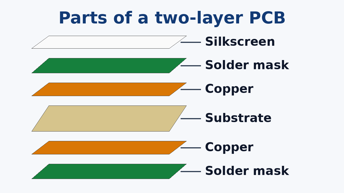
The substrate is the rigid, insulating material the board is built on. On most boards it's an FR-4 type material: woven glass fabric bonded with epoxy resin. It gives the board its stiffness and thickness, keeps the copper layers electrically apart, and largely decides how the board copes with heat.
A two-layer board is usually a single core with copper on both sides. A multilayer board stacks several cores and layers of prepreg (glass cloth with partly cured resin that bonds the stack together in lamination). Our Multilayer PCB Guide explains how cores, prepreg and copper foil are combined.
How it's defined: not in the Gerber files. The material, overall thickness and any requirement such as a higher glass transition temperature go on the fabrication drawing or in the order notes. For material families beyond standard FR-4, our PCB Materials page compares FR-4, high-Tg, RF, flex and metal core options.
2. Copper layers: traces, planes and pours
Copper is what carries current. Each copper layer is patterned into:
- Traces, the narrow paths connecting one point to another.
- Planes, large solid areas usually used for ground or power.
- Pours, copper fills in otherwise empty areas, normally connected to a net such as ground.
Copper thickness is usually stated as weight per area in ounces; 1 oz copper is roughly 35 µm thick. Thicker copper carries more current but needs wider spacing to etch reliably.
How it's defined: one Gerber file per copper layer, plus the copper weight in the notes. On multilayer boards, the layer order must be stated clearly, normally in a stackup table, so that inner layer 2 doesn't end up where layer 3 should be.
3. Holes: plated and non-plated
Holes do several different jobs:
- Plated through-holes have copper plated onto the hole wall so they connect layers. Larger ones take component leads; smaller ones, called vias, only connect layers.
- Non-plated holes have bare walls. They're used for mounting screws, alignment pins and tooling.
- Slots are elongated holes, plated or non-plated, for parts such as connector tabs.
Multilayer boards may also use blind and buried vias, which connect only some layers, and laser-drilled microvias.
How it's defined: NC drill files, usually with plated and non-plated holes in separate files or clearly separated tools. A common beginner mistake is confusing drilled size with finished size. Plating makes a hole smaller, so the drawing should state that sizes are finished hole sizes, and for press-fit or tight-tolerance holes, the tolerance.
4. Pads and annular rings
Pads are the exposed copper areas where components are soldered. Surface-mount pads are flat lands on the outer layers; through-hole pads are rings of copper around a plated hole. The ring of copper between the hole edge and the pad edge is the annular ring. It needs to be wide enough that a slightly off-centre drill still leaves a connection.
Pads that connect to large planes often use thermal reliefs, a few short spokes instead of a solid connection, so that soldering heat doesn't drain away into the plane.
How it's defined: pads are part of the copper Gerbers. Their shape comes from the footprints in your design library.
5. Solder mask: the coloured coating
Solder mask is the thin polymer coating that gives most boards their green (or black, blue, red or white) colour. It covers the copper everywhere except where solder is meant to go. It stops solder bridging between pads during assembly, protects the copper, and adds some insulation between closely spaced conductors.
A few details matter more than they first appear:
- Mask openings around each pad are usually slightly larger than the pad, so small shifts in registration don't put mask on the pad.
- Mask dams, the thin strips of mask between fine-pitch pads, help prevent bridges. If the pads are too close, the dam may not be possible.
- Via tenting covers vias with mask. Whether vias are tented, plugged or left open should be stated.
How it's defined: a solder mask Gerber for each side. These files show the openings, not the coating. A shape in the mask file means "no mask here", which confuses many people the first time they look.
6. Surface finish: the coating on exposed copper
Bare copper oxidises quickly and becomes hard to solder. The surface finish is a thin metallic or organic layer applied to copper that isn't covered by mask, mainly the pads. Common finishes include HASL (lead-free or tin-lead solder levelled with hot air), ENIG (electroless nickel with a thin immersion gold layer), OSP (an organic coating), and immersion silver or tin.
Finishes differ in flatness, shelf life and suitability for fine-pitch parts, wire bonding or edge connectors.
How it's defined: only in the notes or order form. There's no Gerber for the finish; it's applied wherever the mask leaves copper exposed.
7. Silkscreen (legend): the printing on top
The silkscreen, also called the legend, is the printed text and symbols on the outer surface: reference designators such as R12 and U3, polarity marks, pin-1 indicators, part outlines, logos, revision numbers and any required markings.
The factory removes silkscreen from pads and mask openings, because ink on a pad would interfere with soldering. Text that's too small or too thin may not print legibly; the factory's design rules give minimum sizes.
How it's defined: a silkscreen Gerber for each side, plus the colour in the notes.
8. Outline and edge features
The board outline is the shape the board is cut to. Inside and along it there may be:
- Cutouts and internal slots, routed openings in the board.
- V-scores, partial-depth grooves that let boards be snapped apart from a panel.
- Breakaway tabs, small bridges, often perforated, holding routed boards in the panel.
- Castellated holes, plated holes cut in half at the board edge so a module can be soldered onto another board.
- Edge connector fingers, gold-plated contacts along an edge, often with a bevelled edge for insertion.
How it's defined: an outline or mechanical Gerber that shows only the board edge and cutouts, plus notes or a panel drawing for V-scores, tabs, bevels and plating.
9. Fiducials, tooling holes and test points
These small features help the board through manufacturing and test:
- Fiducials are bare copper dots with a mask-free area around them. Assembly machines use them to locate the board precisely.
- Tooling holes hold the board or panel in place during assembly and test.
- Test points are exposed pads where probes can touch nets for electrical testing.
They're part of the copper, mask and drill data, and are worth planning during layout rather than adding at the end.
10. The paste layer, which isn't part of the board
Design tools also output a solder paste layer. It doesn't become part of the bare board; it's used to make the stencil that prints solder paste onto the pads during assembly. It belongs with the assembly files rather than the fabrication files.
11. The part you can't see: the drawing and stackup
Several things that define the board never appear as geometry: material, thickness, copper weights, finish, mask and silkscreen colours, impedance requirements and the acceptance class (IPC-6012 sets out performance classes for rigid boards). They live on the fabrication drawing, in the stackup table, or in the order notes.
If one of these is missing, the factory either asks in an engineering question or applies its default. Our Manufacturing Files page lists the Gerber, drill, stackup and assembly files to prepare with an order.
A quick reference
| Part | Main job | Defined by |
|---|---|---|
| Substrate | Stiffness, insulation, heat resistance | Drawing or notes |
| Copper layers | Carry current and signals | Copper Gerbers + copper weight note |
| Holes and vias | Connect layers, mount parts | Drill files |
| Pads | Solder joints | Copper Gerbers |
| Solder mask | Prevent bridges, protect copper | Mask Gerbers (openings) + colour note |
| Surface finish | Keep pads solderable | Notes only |
| Silkscreen | Identify parts and polarity | Silkscreen Gerbers + colour note |
| Outline and edges | Board shape, panel separation | Outline layer + notes |
| Fiducials, test points | Assembly alignment, testing | Copper, mask and drill data |
Once you can name each part and know where it's defined, a board stops looking like a maze. It becomes a set of layers, each with a job, and each described somewhere in the data you send.