

"Better signal transmission" on a PCB usually means one of two things. Either the signal arrives with the wrong shape because of reflections, crosstalk or timing skew, or it arrives too small because the board absorbed too much of it on the way. The first group is mostly about impedance control and layout discipline. This article is about the second: loss.
As data rates rise, loss becomes the limit that layout neatness cannot fix. A perfectly matched 50 ohm trace still attenuates the signal more with every centimetre, and more at higher frequencies than at lower ones. The receiver can equalise some of that, but only up to a point. The practical tool for managing it is a channel loss budget: an allowance, in decibels at a stated frequency, that the transmitter, package, connectors, vias and board traces have to share.
From the factory side, we see the consequences of loss budgets in the materials, copper foils and drilling notes on the drawings we receive. Here is how the budget is spent on the board, and which choices buy it back.
The budget, briefly
Interface specifications for fast serial links typically define how much insertion loss the channel may have at a reference frequency, usually related to half the data rate (the Nyquist frequency). Whatever the silicon and connectors consume, the rest is available for the PCB. A long trace on a large board can use up most of it on its own.
On the board, the loss has three main sources, and they behave differently:
- Dielectric loss, set by the laminate's dissipation factor (Df), rises roughly in proportion to frequency.
- Conductor loss, set by the copper geometry and surface, rises with frequency as current crowds towards the copper surface (the skin effect), and is made worse by rough copper.
- Discontinuity loss at vias, connectors and pads, where reflections and resonances take energy out of the signal at specific frequencies.
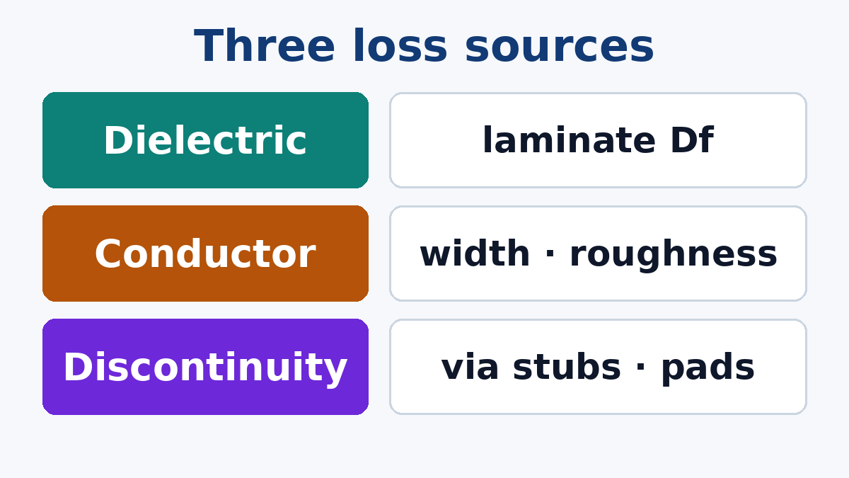
Which one dominates depends on the frequency and the build. On standard FR-4 at moderate frequencies, dielectric loss is often the larger part. On a low-loss laminate, conductor loss and roughness become relatively more important, which is why changing only the laminate sometimes gives less improvement than expected.
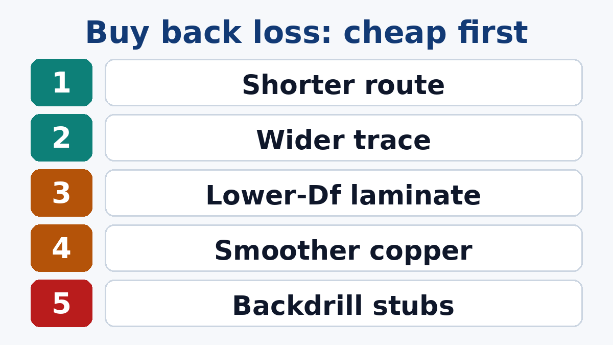
Lever 1: Length, before anything else
Trace loss scales with length. The cheapest decibels are the ones you never spend: place the high-speed devices and connectors so that the critical links are short, and avoid routing them the long way round to reach a convenient layer. Once the layout has fixed a long route, every remaining lever costs money.
Lever 2: Trace width and dielectric thickness
Conductor loss falls as the trace gets wider, because there is more copper surface to carry the current. But at a fixed impedance, a wider trace needs a thicker dielectric to its reference plane. So the real trade is between loss and board thickness, layer count and routing density. Narrow traces in a thin, dense stackup are convenient for routing and costly in loss.
This is one reason why impedance and loss have to be designed together. An Impedance Control PCB process holds the impedance to tolerance; it does not decide whether the geometry that achieves it is a low-loss one.
Lever 3: Laminate dissipation factor
Moving from a standard FR-4 to a mid-loss or low-loss laminate reduces dielectric loss directly. A few practical points that often get missed:
- Use data at your frequency. Dk and Df vary with frequency and resin content. A datasheet value at 1 GHz is not the value at the Nyquist frequency of a fast link. Model with the supplier's frequency-dependent data for the actual glass style and resin content in your stackup.
- Prepreg counts too. In a stripline, the signal sees both core and prepreg. Specifying a low-loss core with a standard prepreg wastes part of the benefit.
- Hybrid stackups put low-loss material only on the layers that carry the critical signals, with standard material elsewhere. That can reduce cost, but it adds lamination and drilling considerations that should be discussed with the fab before layout.
- Lock the material. If the material is part of the loss budget, the drawing should name it or define its required properties, and should say whether substitutes are acceptable.
Lever 4: Copper roughness
Copper foil is rough on the side that bonds to the dielectric, because that roughness helps adhesion. At high frequencies the current flows in a thin layer near the surface, so it follows the rough profile and travels further, which increases loss. Low-profile and very-low-profile foils reduce this effect.
Two notes from the production side. First, the inner-layer oxide or bonding treatment also modifies the copper surface, so the foil datasheet is not the whole story. Second, smoother copper bonds less aggressively to the resin, so material systems designed for low-loss work pair the foil with suitable resin and treatment. Specify the foil type together with the laminate system rather than as an independent choice.
Lever 5: Vias and their stubs
A through-hole via that carries a signal from layer 1 to layer 3 of a thick board leaves the rest of the barrel hanging below as a stub. The stub behaves like an open-ended transmission line, and it resonates when its length equals a quarter of the wavelength in the dielectric:
f(resonance) ≈ c / (4 × stub length × √Dk_eff)
Near that frequency the stub removes a large amount of energy from the signal, and well below it the stub still adds capacitance and reflections. As an illustration of the arithmetic, a 1.5 mm stub in a material with an effective Dk around 3.8 resonates near 26 GHz. A link whose energy extends into that region will see a notch in the channel response.
The ways to deal with stubs, roughly in order of cost:
- Choose the layers. Routing a critical signal from the top layer to a layer near the bottom uses most of the via barrel and leaves a short stub.
- Backdrilling. After plating, the unused portion of the barrel is drilled out from the opposite side with a slightly larger drill. Backdrilling is controlled-depth drilling, so it leaves a small residual stub and needs a defined tolerance. The drawing should state which vias are backdrilled, from which side, the layer that must not be cut, and the maximum remaining stub length.
- Blind and buried vias, or HDI structures, avoid the stub altogether but change the fabrication route and cost considerably.
Pads, antipads and the transition into connectors also matter. A via is a short section of transmission line with its own impedance; antipad size and the placement of ground vias next to signal vias keep that impedance close to the trace's.
Lever 6: Microstrip or stripline
Outer-layer microstrip has part of its field in air, which lowers the effective dielectric loss, but it is exposed to solder mask, surface finish and the environment, and it radiates and picks up more noise. Surface finish on exposed traces and pads can add loss of its own. Stripline is better shielded and more predictable, with fully embedded dielectric loss. For most long high-speed links, stripline on well-chosen material is the predictable option, with short microstrip breakouts at the devices.
Verifying loss on the board
Impedance coupons are routine. Loss coupons are less common, but for designs where loss is the limiting factor, they are the only way to show that the laminate, foil and process actually delivered the budget.
IPC-TM-650 method 2.5.5.12 describes several ways to measure signal loss on printed boards, including time-domain methods suitable for production such as SET2DIL and a frequency-domain method using a vector network analyser. Multi-length coupon methods such as Delta-L, reflected in IPC-TM-650 2.5.5.14, are widely used to separate the loss per unit length from the launch and via effects. If you need loss measurement, agree the method, coupon design, layer, frequency points and acceptance limit with the fab before the order. "Low loss" on a drawing cannot be tested.
What to put on the fab drawing
- Laminate and prepreg system, or required Dk and Df at a stated frequency, and whether substitutes are allowed
- Copper foil type for the critical layers
- Stackup with dielectric thicknesses, and which layers carry loss-critical signals
- Impedance targets and tolerances
- Backdrill callouts: via list, drill side, must-not-cut layer, maximum residual stub
- Loss test requirement, if any: method, coupon, frequency and limit
If your board's loss budget is tight, send us the stackup and the critical-link requirements early. Our engineers can tell you which materials and foils we can source for that stackup, how backdrilling would be specified on your thickness, and what loss verification we can provide. For links that also run into the RF range, our High Frequency PCB team can review the material choice with you.