
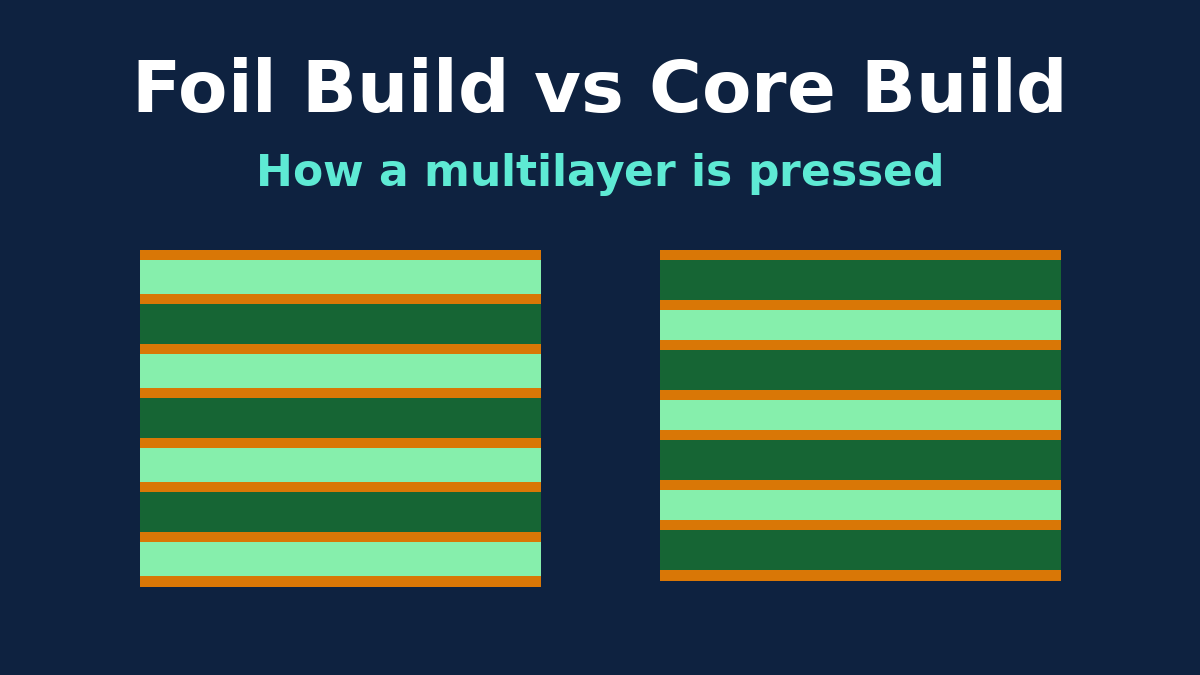
A stackup drawing shows layers in order: copper, dielectric, copper, dielectric. What it doesn't always show clearly is how those layers are physically put together in the press. Two boards with the same layer count, the same finished thickness and almost the same drawing can be built in different ways, and the difference affects cost, impedance control on the outer layers and sometimes flatness.
This article is about that physical construction for standard through-hole multilayers, the kind IPC-2222 calls Type 3 (no blind or buried vias). It covers the two ways the outer layers are formed, how to tell which one a factory's stackup proposal is using, when it's worth asking for the less common one, and what happens when a design calls for an odd number of layers. Choosing the layer count and the signal and plane order is covered in our multilayer stackup and classification articles.
Three materials go into the press
Every rigid multilayer is made from the same three ingredients:
- Cores. Fully cured glass-epoxy laminate with copper on both sides. Inner-layer circuits are imaged and etched on cores before lamination.
- Prepreg. Glass cloth impregnated with partly cured resin. In the press it softens, flows into the gaps between copper features, then cures and bonds everything together.
- Copper foil. Plain foil, with no dielectric attached, laid on the outside of the stack.
How these are arranged at the top and bottom of the stack is what separates the two constructions.
Foil build: the mainstream construction
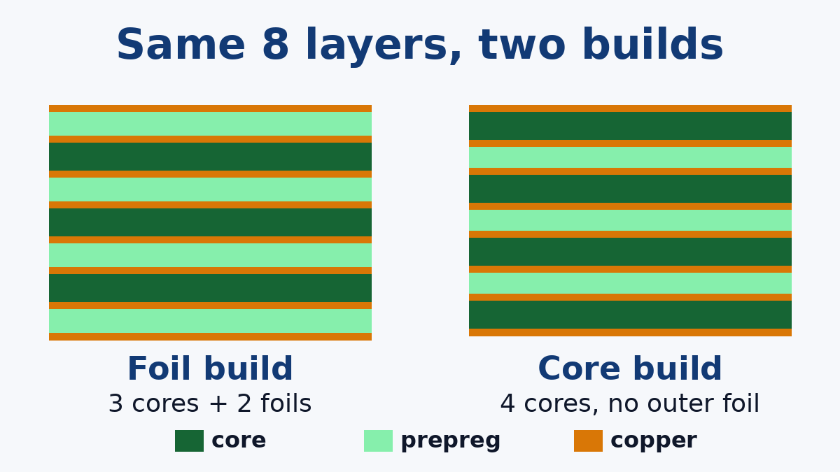
In a foil build, the inner layers are all on cores, and the outermost layers are plain copper foil laid on prepreg. An eight-layer foil build typically uses three cores (carrying layers 2–3, 4–5 and 6–7), prepreg between them, and a sheet of foil on each side that becomes layers 1 and 8.
After pressing, the outer foil is drilled through with the rest of the board, plated when the holes are plated, then imaged and etched into the outer circuit.
Why it's the default:
- Fewer cores, so lower material cost. Foil and prepreg cost less than an extra pair of cores.
- Fewer process steps. Every core has to be imaged, etched, inspected and surface-treated before lamination. Fewer cores means less of that work and less handling.
- Flexible outer dielectric. The thickness between layers 1 and 2 is set by the prepreg chosen, so the factory can tune it with different prepreg styles.
- Thin starting foil. Outer layers can start from thin foil, which leaves room for plating while still etching fine features.
The trade-off is that the dielectric under the outer layers is prepreg. Its pressed thickness depends on resin flow and on how much copper sits on layer 2, so it has a wider tolerance than a core of the same nominal thickness.
Core build: when the outer dielectric must be a core
In a core build, sometimes called cap lamination, the outer layers come from cores rather than foil. The same eight-layer board uses four cores: layers 1–2, 3–4, 5–6 and 7–8. Before lamination, only the inward-facing side of each outer core is imaged (layers 2 and 7). The outward side stays as plain copper until after pressing and plating, when it's imaged into layers 1 and 8.
What that buys:
- Tighter dielectric under the outer layers. The layer between 1 and 2 is a cured core, with a thinner thickness tolerance than pressed prepreg. If outer-layer impedance has to be held tightly, that matters.
- A specific material on the outside. In hybrid builds, a low-loss RF core can be placed directly under the top layer for microstrip lines while the rest of the board stays FR-4. That's a core build at least on that side.
- Different flatness behaviour. Some designs, particularly with heavy copper, use outer cores to improve surface flatness or balance.
What it costs:
- More cores and more handling. The extra cores are imaged on one side before lamination, and their untouched outer copper has to be protected through inner-layer processing, which adds steps and scratch risk.
- Less freedom on the outer copper. The starting outer copper is whatever the core is clad with.
For most boards, a foil build does everything needed. A core build is something to ask for with a reason, not by default.
How to tell which build a stackup sheet shows
A factory's stackup proposal usually lists each dielectric as either core or prepreg, with a material name and pressed thickness. A quick read:
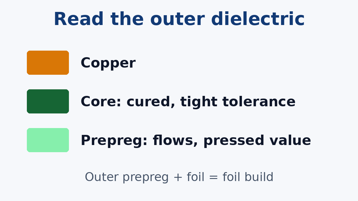
- Outer dielectrics labelled prepreg, outer copper labelled foil: a foil build.
- Outer dielectrics labelled core: a core build, at least on that side.
- Prepreg thickness given as a pressed value: good. Prepreg shrinks in the press as resin fills the copper gaps, so the nominal sheet thickness isn't the finished value, and impedance should be calculated from the pressed value.
- Copper weights listed per layer, with outer layers shown as starting foil plus plating: normal for a foil build.
If your impedance model assumed a core under layer 1 and the proposal shows prepreg, the numbers will differ. Rerun the model with the factory's values rather than asking the factory to match yours.
When to ask for a core build
Reasons that justify it:
- Outer-layer controlled impedance with a tighter tolerance than the foil build can comfortably hold on your stack.
- A hybrid design that needs a particular laminate directly under the outer layer.
- A stack where symmetry or flatness is hard to achieve any other way, which the factory can usually advise on.
For outer-layer impedance, it's often enough to state the requirement and tolerance and let the factory propose the construction. Our Impedance Control PCB review starts from the requirement rather than a fixed build, and a core build is one of the options when it's needed.
Odd layer counts: possible, rarely worthwhile
Designs sometimes come out at five, seven or nine layers. They can be built, but an odd count doesn't sit naturally in the core-and-prepreg system, because every core carries two copper layers. Factories handle it in a few ways:
- Build the next even count and remove one layer's copper. A five-layer board is made as six layers, with one copper layer etched away completely. The material and process are those of a six-layer board.
- Use a core with copper on one side only, or etch one side of a core bare. The bare side needs treating so the prepreg bonds well to it.
- Accept an asymmetric stack, which raises the risk of bow and twist after lamination and reflow.
None of these makes the board meaningfully cheaper than the next even count, and the asymmetric options add warpage risk. In practice, it's usually better to use the extra layer: turn a five-layer design into a six-layer one and give the spare layer to ground, which improves return paths and shielding at little extra cost. Our 6-Layer PCB page compares common six-layer stackup arrangements if you're deciding what the extra layer should do.
Keep the stack symmetrical either way
Whichever construction is used, a stack should mirror about its centre: matching dielectric thicknesses, matching copper weights and similar copper coverage on mirrored layers. A stack that's heavy on one side, such as a thick-copper power layer near the top with only thin signal layers near the bottom, shrinks unevenly as it cools after pressing and can come out bowed. If your design needs an unbalanced copper distribution, mention it, so the factory can add copper balancing in unused areas or adjust the construction.
What to put on the drawing
- Layer count, finished thickness and tolerance.
- The layer order, with which layers are signal and which are planes.
- Copper weights per layer, stating whether outer weights are starting or finished.
- Impedance requirements by layer, with reference planes and tolerance.
- Any construction requirement, such as a core under a particular outer layer, with the reason, so alternatives can be discussed.
- Whether the factory may propose its own construction for approval. For most boards this is the fastest route to a buildable stack.
For a broader overview of the materials and process steps behind these builds, see our Multilayer PCB Guide. Whatever the layer count, agreeing the construction before layout is finished keeps the impedance model, the drawing and the board in agreement.