
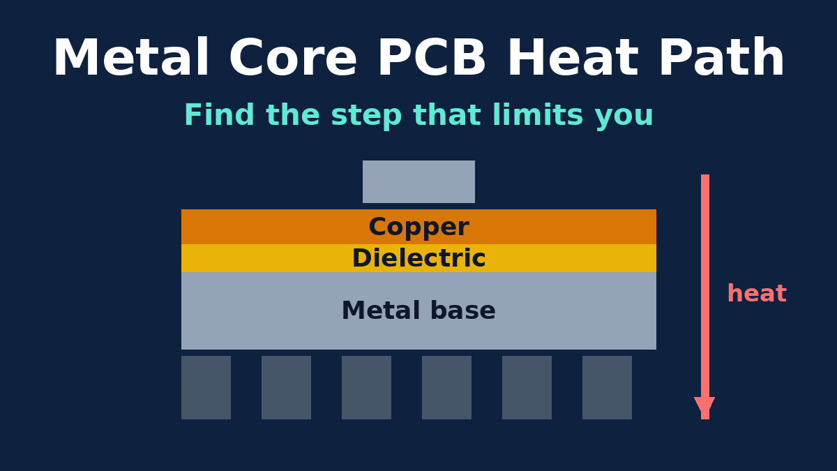
"Use a metal core board" is good advice for a hot LED or a power MOSFET, but the board doesn't make the part cool. It gives the heat a path, and the part runs as hot as the worst step on that path allows. When a prototype runs hotter than expected, the fix is usually not a better aluminium grade. It's finding which step is eating the temperature budget.
This article follows the heat from the component to the air, one layer at a time, and shows how to put rough numbers on each step. Which products suit metal core boards, and what each application asks for beyond cooling, is covered in our companion article on metal core PCB applications. Here we stick to the physics and to the details on the drawing and the assembly that change it.
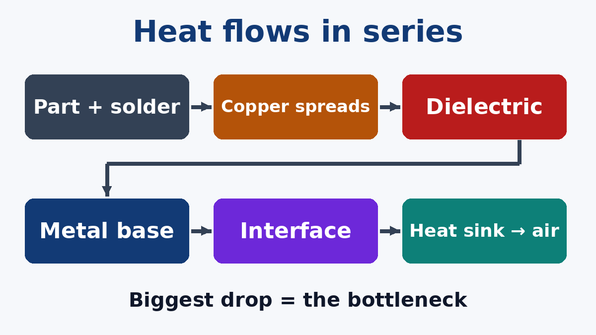
Think in thermal resistance, not conductivity
A datasheet gives thermal conductivity, k, in W/m·K. That's a property of the material. What sets the temperature is thermal resistance, which depends on the material and its geometry too. For a flat layer with heat flowing straight through it:
R = t / (k × A)
Here t is the layer thickness, A is the area the heat actually flows through, and R comes out in K/W. Multiply R by the power through that layer and you get the temperature drop across it. Stack the layers in series and the drops add up:
Tjunction ≈ Tambient + P × (R1 + R2 + R3 + …)
This is a screening model. It ignores the fact that heat spreads sideways and that real interfaces are imperfect. But it's enough to show which layer dominates, and that's the question that matters.
A useful habit is to separate thickness and k from area. Thickness divided by k gives an area-specific resistance in mm²·K/W. For example, a 100 µm dielectric at 2 W/m·K works out to 50 mm²·K/W. Divide by the area under the heat source and you have that layer's resistance. Some dielectric datasheets quote this figure directly, often as °C·cm²/W or °C·in²/W, and for comparing dielectrics it's more honest than k alone because thickness is already included.
Step 1: Component to pad
The heat starts at the die, crosses the package (the datasheet's junction-to-case or junction-to-solder-point resistance), then the solder joint, and reaches the copper pad.
The board can't change the package. The joint, though, is worth attention. Voids in the solder under an exposed thermal pad cut the area the heat passes through, and on a metal core board that's often the first place the path narrows. The stencil design under large thermal pads (usually a segmented "windowpane" opening rather than one big aperture) and the reflow profile control voiding. If the thermal pad matters, ask for voiding to be checked by X-Ray Inspection on first articles. Visual inspection can't see under the part.
Step 2: Copper spreading, the cheapest lever
This step is the one designers most often underrate. The dielectric below is the weakest layer, and its resistance is inversely proportional to area. So whatever spreads the heat sideways before it reaches the dielectric directly lowers that resistance.
That job falls to the copper layer. A small LED thermal pad connected to nothing pushes all its heat through a few square millimetres of dielectric. The same pad tied into a wide copper area lets the heat fan out first, so it crosses the dielectric through a much larger footprint.
Illustrative arithmetic, using the 50 mm²·K/W dielectric above and a part dissipating 5 W:
- Heat confined to a 25 mm² pad: 50 / 25 = 2 K/W, so about 10 °C across the dielectric.
- Heat spread over an effective 100 mm²: 0.5 K/W, so about 2.5 °C.
These numbers are geometry examples, not product data. Real spreading depends on copper thickness and the pattern, and thin copper only spreads well over short distances. The direction is reliable, though. Heavier copper and generous copper around hot pads (connected to the thermal pad, not isolated islands) usually buy more than a dielectric upgrade does. Copper weight on metal core boards also affects etching and minimum spacing, so check what's achievable against our Copper Thickness Capability when you choose it.
Step 3: The dielectric, where most of the board's resistance sits
The dielectric has to insulate the circuit from the base and pass heat at the same time. Thermally conductive dielectrics are filled with ceramic particles to raise k, but even good ones remain far below the metals around them. Copper is close to 400 W/m·K and common aluminium alloys are roughly 130 to 230 W/m·K, while thermal dielectrics are usually quoted in the low single digits. That's why, inside the board itself, this thin layer typically carries most of the temperature drop.
Two things to know when comparing dielectrics:
- Thinner conducts better but insulates less. Halving the thickness halves the thermal resistance, and it also lowers breakdown margin. On mains-connected or high-voltage designs, the hipot requirement sets the minimum thickness first, and the thermal choice comes after.
- The k value depends on how it was measured. Steady-state methods such as ASTM D5470 measure through-thickness heat flow between hot and cold plates. Laser flash (ASTM E1461) measures diffusivity and calculates conductivity. It's intended for homogeneous materials, which a filled dielectric bonded between metals isn't. The two can give different numbers for the same product. IPC-TM-650 2.4.54, written for metal-based printed boards, measures the whole copper–dielectric–metal specimen and reports an apparent conductivity that includes the contact resistance at each interface. When two quotes show different k values, check which method each uses before concluding one dielectric is better.
Step 4: The metal base
Once the heat is in the base, it moves easily. A 1.5 mm aluminium base at about 150 W/m·K, with the heat spread over 400 mm², contributes roughly 0.025 K/W (again illustrative), which is tiny next to the dielectric. The base's real job is spreading the heat so that it leaves through the full back surface.
That's why switching from aluminium to a copper base often changes less than expected. Copper spreads better and helps when the heat sources are small and very concentrated, but it doesn't touch the dielectric resistance. The construction that does is a copper base with a raised pedestal under an electrically neutral thermal pad, so the part bypasses the dielectric entirely. It works, but it's a different, costlier build with its own design rules. For standard Aluminum PCB builds, the dielectric and the spreading above it remain the main levers.
Step 5: Base to heat sink, the step outside the board
This is the step most often left out of the thermal estimate, and it's frequently the largest. A metal core board pressed against a housing or heat sink touches it only at high points. The gaps are air, and air is a very poor conductor. A thermal interface material fills them. Thermal grease, gap pads and phase-change materials all have their own resistance, which depends on the bond line thickness and the clamping pressure.
Illustrative: a 0.2 mm interface at 1 W/m·K across 400 mm² adds 0.5 K/W. That's as much as the well-spread dielectric in step 2.
Board-side details affect this step:
- Flatness. A board that bows after reflow lifts away from the heat sink in the middle, often right under the hottest parts. State a flatness requirement if the mounting is critical.
- Mounting hole edges. Burrs or raised edges from drilling and routing hold the board off the surface. They should be removed, and it's worth asking how.
- Screw placement and torque. Screws near the hot parts clamp the interface where it matters. Over-tightening can bow the board or crack ceramic packages.
Step 6: Heat sink to air
Finally, the heat has to leave by convection and some radiation. With natural convection and a small heat sink, this step can dominate everything above it. In that case, no change to the PCB will make much difference, and the answer is a bigger heat sink, fins or airflow. Before spending money on a premium dielectric, check that this step isn't the real limit.
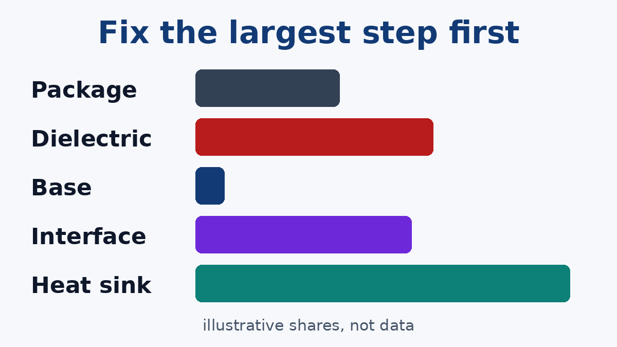
Putting it together: the budget
Start from the allowed junction temperature, subtract the worst-case ambient, and divide by the power. That's your total thermal resistance budget in K/W. Then fill in each step: the package figure from the datasheet, and estimates for the joint, the dielectric over its effective area, the base, the interface and the heat sink. Whichever step takes the largest share is where effort pays off. Improving any other step barely moves the junction temperature.
For final designs, a thermal simulation that models spreading properly is worth doing. It needs the layer thicknesses and the dielectric's apparent conductivity as inputs.
Checking a prototype: measure where the temperature drops
The simplest diagnostic on a powered prototype is to measure temperature at several points along the path:
- Component case or solder point. Use a fine thermocouple bonded to the case. For LEDs, the junction can be estimated from the forward-voltage shift, the electrical test approach described in JEDEC JESD51-1.
- Board surface next to the part, and on the back of the base directly underneath it.
- The heat sink near the board, and the ambient air.
The biggest temperature difference between two neighbouring points shows which step is the bottleneck. A large drop between the base and the heat sink points to the interface or mounting, not the dielectric. A large drop from the case to the board points to the joint, voids or a pad that is too small.
If you use an infrared camera, bare aluminium and shiny copper have low emissivity and read far cooler than they are. Put a small piece of high-emissivity tape or a dot of matt black paint on each spot you measure.
What to put on the drawing and RFQ
So that the board you receive matches the thermal model:
- Dielectric thermal conductivity and the test method, the dielectric thickness, and the required breakdown or hipot voltage.
- Copper weight on the circuit layer.
- Base material, alloy if it matters, and thickness.
- Flatness requirement and mounting hole edge condition, if the board is clamped to a heat sink.
- For assemblies, the voiding requirement under thermal pads and how it will be inspected.
When we review a Metal Core PCB order, we check these items against the files and ask about anything missing rather than assume. We can't tell you the heat sink is too small, though. Only your thermal budget can, so it's worth running before the board is the thing that gets changed.