

The usual comparison of microstrip and stripline is about electromagnetics: one line sits on the surface with part of its field in air, the other is buried between two planes and shielded. That's the right starting point for choosing between them, and it's well covered. What gets less attention is how the two behave once a factory builds them. They're sensitive to different process variables, they need different things on the drawing, they cost different amounts in RF material, and they're verified in different ways.
This article looks at microstrip and stripline from the production side. It assumes you know what each structure is. If you're working through insertion loss on long high-speed links, our channel loss budget article covers that separately. Here the questions are which line is easier to hit on target, which one costs more, and what to specify so the board you receive matches the field solver.
Why the same target lands differently in production
A field solver gives you a width for 50 Ω from four main inputs: trace width (and its etched shape), copper thickness, dielectric height to the reference plane, and the dielectric constant. Every one of those is a manufactured quantity with its own tolerance. Microstrip and stripline don't just use different values. They draw those values from different parts of the process, and some of those parts are better controlled than others.
What moves a microstrip
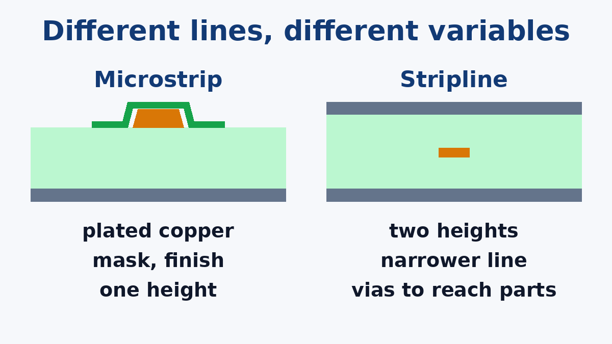
Copper thickness and etched width on the outer layer. Outer layers start as thin foil and are then plated up when the through holes are plated. The final copper thickness depends on plating, which isn't perfectly uniform across a panel. The etched width depends partly on that thickness, because thicker copper etches with more sideways undercut and a more trapezoidal shape. So an outer-layer trace carries two linked sources of variation that an inner-layer trace largely avoids.
The dielectric under it. A microstrip has only one dielectric layer to its reference plane. In a typical multilayer built with foil on the outside, that layer is prepreg, whose pressed thickness depends on resin flow and on how much copper is on the layer beneath. If the microstrip is referenced across a core instead, the height is more tightly controlled.
Solder mask. If mask covers the line, it raises the effective dielectric constant around the trace, which lowers the impedance, typically by a few ohms depending on mask thickness and material. Mask thickness isn't perfectly uniform: it's usually thinner on top of the trace and thicker in the gaps, which matters most for edge-coupled differential pairs. The solver model should include the mask if the line will be masked, with the factory's typical mask thickness.
Surface finish, if the line is left bare. Some RF designs open the mask over the line to avoid mask loss and variation. The trace then gets the board's surface finish. A nickel-based finish such as ENIG puts a layer of nickel on the trace surface, where high-frequency current flows, and nickel adds conductor loss. Immersion silver, OSP or a selective finish avoid that, each with its own handling and shelf-life trade-offs. Deciding mask-on or mask-off for RF lines is a design decision, and it changes both the impedance and the finish choice.
Its surroundings. A microstrip's field reaches above the board, so a shield can, conformal coating or nearby enclosure wall changes it. That's not a fabrication variable, but it's a reason a microstrip can measure differently in the product than on the bare board.
What moves a stripline
Two dielectric heights, not one. A stripline sits between two reference planes, so its impedance depends on both dielectric layers and on where the trace sits between them. At least one of those layers is usually prepreg, and its pressed thickness depends on the copper density of the layers on either side. If the trace isn't centred (an asymmetric or offset stripline), the impedance depends on each height separately. This is why stripline designs have to be modelled with the factory's pressed thicknesses, not the nominal prepreg thickness from a datasheet.
Narrower lines. For the same impedance on the same stackup, a stripline is narrower than a microstrip, because the field sits entirely in dielectric and there are two planes nearby. A fixed etching tolerance is a larger fraction of a narrow line. As an illustration only, a ±0.025 mm width variation is about ±17% of a 0.15 mm trace but about ±8% of a 0.3 mm trace. If a stripline comes out very narrow, increasing the dielectric heights to widen it often makes the impedance easier to hold.
Inner-layer copper, which helps. Inner layers of a standard multilayer aren't plated, so their copper thickness is the foil thickness, and they etch with less undercut. In that respect, stripline is easier to control than microstrip. (Sequential builds with buried vias do plate some inner layers, which brings the outer-layer variation back.)
No mask, no finish, no environment. None of the surface effects above apply. Once the stackup is right, a stripline tends to be the more predictable line.
Vias: the cost stripline doesn't show on the cross-section
Every RF component is on the surface. A microstrip can run from one part to the next without leaving the outer layer. A stripline needs at least two layer transitions, one down and one back up, and each via is a short section of different impedance with a stub below the layer it connects to. At low frequencies this is negligible. As frequency rises, transitions need care: ground vias placed close beside the signal via to carry the return current between planes, antipads sized for the via's impedance, and on thicker boards, backdrilling to remove the unused stub.
This is the stripline's hidden cost, in design time, in extra drilling and possibly backdrilling. It's also why many RF designs use microstrip near the components and stripline only for longer runs that need shielding.
Material cost: one RF layer or two
If the RF path needs a low-loss laminate rather than FR-4, the structure decides how much of it you buy.
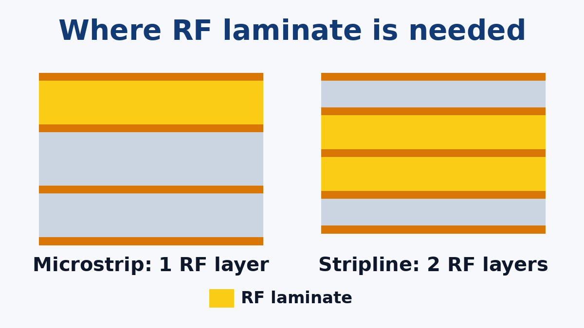
A microstrip needs good material only between the trace and its reference plane. A common hybrid stackup puts a single RF laminate core under the top layer and builds the rest of the board from FR-4. The expensive material is limited to one layer.
A stripline's field fills the dielectric on both sides of the trace, so both layers need the RF material to get its full benefit. That usually means more RF laminate and an RF-compatible bonding layer, with more lamination considerations when different material systems are pressed together. For boards where the RF lines are short, the microstrip hybrid is often the lower-cost route. If you're weighing a hybrid build, our High Frequency PCB page describes how we review RF and hybrid material choices during DFM.
Grounded coplanar waveguide: an etched gap joins the list
Grounded coplanar waveguide is an outer-layer line with ground copper beside it as well as below. Its impedance depends on the gap to that side ground as well as on the width and height, and the gap is an etched dimension too. It carries all the outer-layer variables of a microstrip, plus gap tolerance. In return, it confines the field better and is less affected by neighbouring traces. If you use it, model it as coplanar from the start. A microstrip width with ground copper poured close beside it is no longer the impedance you calculated.
How each one is verified
Controlled impedance is normally verified with TDR on test coupons built into the production panel. The coupon only represents the board if it reproduces the structure: the same layer, the same reference planes, the same mask condition and the same trace geometry. For a stripline, the coupon is effectively the only practical evidence, because the line inside the board can't be probed. For a microstrip, it's sometimes possible to probe the line on the board itself, which helps when troubleshooting a prototype.
When you order controlled impedance, it helps to list each impedance requirement with its layer, reference planes, structure type and tolerance, and to let the factory adjust widths slightly to hit the target on its process. Our Impedance Control PCB page outlines the stackup review and coupon approach we use for these orders.
A factory-side comparison
| Microstrip | Stripline | |
|---|---|---|
| Copper thickness | Foil plus plating, more variation | Foil only on standard builds |
| Dielectric heights in the model | One | Two, plus trace position |
| Solder mask effect | Yes, if masked | None |
| Surface finish effect | Yes, if bare | None |
| Typical width for a given impedance | Wider | Narrower, tolerance is a bigger fraction |
| Layer transitions to reach parts | None | At least two vias per line |
| Low-loss material needed | One layer | Both sides of the trace |
| Verification | Coupon, sometimes probed on board | Coupon |
What to put on the drawing
- The stackup, with which layers carry controlled-impedance lines and their reference planes.
- Each impedance requirement: value, tolerance, structure (microstrip, stripline, coplanar, differential), layer and nominal geometry.
- Whether RF lines are covered by solder mask or left open, and the surface finish on any open lines.
- Material for the RF layers, or required Dk and Df at a stated frequency, and whether substitutes are allowed.
- Whether the factory may adjust trace widths to meet impedance, and by how much.
- Backdrill requirements, if any, for stripline transitions.
Send the stackup with your first quote request. Most impedance problems we see come from a model built on nominal values the factory never agreed to, and those are far easier to fix before layout is finished than after the first coupons come back.