
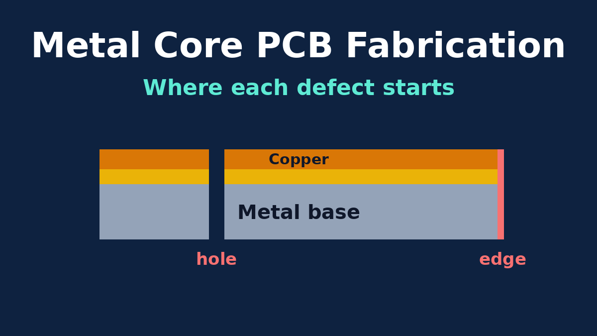
Most metal core PCB problems that reach a customer show up in one of two ways: a board that leaks or breaks down during hi-pot testing, or a board that looks wrong (a stained aluminium back, a burr at a mounting hole, a crack along the edge). Almost none of them start at the step where they're found. They start earlier, at a drill, an etching line, a chemical bath or a router, and they're simply discovered at the end.
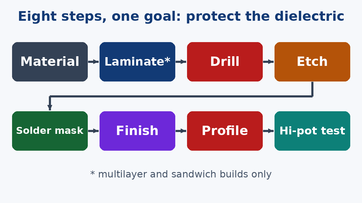
This article walks through how a metal core board is made in a factory, in the order it happens, and notes at each step what can go wrong and why. If you know where a defect comes from, you can read a failure report properly, ask a supplier the right question, and avoid a few layout choices that make the process harder than it needs to be. Thermal design and the choice of applications are covered in our other metal core articles. Here the subject is the production line.
The one thing every step is protecting
A standard FR-4 board is insulating all the way through. A metal core board isn't. Under the copper circuit there's a thin dielectric layer, and under that is a slab of aluminium or copper that conducts electricity as well as heat. The whole board's electrical safety depends on that dielectric staying intact everywhere, including at every hole and along every edge.
That's why metal core fabrication looks like normal PCB fabrication with extra caution added at almost every stage. A scratch that would be cosmetic on FR-4 can be a breakdown path on a metal core board. A burr that would be trimmed off FR-4 can bridge copper to the base. Keep this in mind through the steps below, because most of the special handling comes back to it.
Step 1: Starting material and panel cutting
Single-layer aluminium boards, the most common metal core build, usually start from a ready-made laminate: copper foil, thermal dielectric and metal base, already bonded by the laminate maker. The factory cuts it into working panels. More complex builds, such as a multilayer FR-4 circuit bonded to a metal base or a metal core in the middle of the stack, involve lamination in the factory, which is the next step.
The laminate arrives with a protective film on the metal side. That film is the metal's protection through most of the process, and it stays on until a step specifically needs it off. Cutting must leave clean panel edges. Rough edges shed metal chips, and loose aluminium particles are exactly the kind of foreign material that later ends up pressed into a dielectric or trapped under solder mask.
Defects that start here: wrong dielectric grade or thickness (a material control issue, not a process one), damaged protective film, chips and dust on the panel.
Step 2: Lamination (multilayer and sandwich builds only)
When a factory bonds layers itself, as with a multilayer circuit on a metal base or a metal core inside the stack, the inner circuit layers are imaged and etched first, and then everything is pressed together before the main drilling. The metal surface has to be prepared so that the dielectric grips it. Copper is typically treated with an oxide or similar treatment and aluminium is anodised or mechanically roughened. After preparation, the bonding surfaces must not be touched by bare hands. Skin oil is enough to weaken the bond.
Then comes pressing. Resin flow, pressure and the press cycle decide whether the dielectric fills evenly without voids, and whether the finished board is flat. The metal and the dielectric have different expansion rates, so an unbalanced stack can bow as it cools.
Defects that start here: voids, weak bonding that shows up as delamination after reflow, uneven dielectric thickness, bow.
Step 3: Drilling
Holes in a metal core board go through metal, so drilling is closer to machining than to drilling glass-epoxy. Panels are drilled copper side up, usually stacked low or one per stack, with an entry and backup sheet. Copper side up matters: a drill pushes a burr out of the exit side, so this places any burr on the metal face rather than on the circuit side next to the copper.
Drill wear is the main variable. Metal blunts bits much faster than FR-4, and a blunt bit tears rather than cuts, leaving a raised burr around the hole and a rough wall. A burr on the metal side can stop the board sitting flat on a heat sink. A burr or smeared metal near the dielectric at the hole wall shortens the insulation distance between the copper pad and the base.
Plated through holes are a special case. On a board with circuitry on both sides of a metal core, a plated hole can't simply be drilled and plated, or it would short every layer to the core. The usual method is to drill an oversized clearance hole in the metal first and fill it with insulating resin, either as a separate fill or by resin flowing in during lamination. The final hole is then drilled through the cured resin and plated, so the plating sits inside a resin sleeve. Each extra drilling and filling step is another chance for voids in the resin or misregistration between the two holes, so plated holes through metal add cost and risk. If your design doesn't need them, a single-layer layout avoids them entirely.
Defects that start here: hole burrs, rough or oversized holes, voids in resin-filled holes, cracked dielectric around the hole.
Step 4: Imaging and etching the circuit
The circuit layer is imaged and etched much as on any board, but only on the copper side. The protective film on the metal side stays in place, and only the copper face is brushed or cleaned before the dry film goes on.
The rule that matters most here is about rework. If copper residue is left between features after etching, it mustn't be scraped off with a blade. The dielectric directly underneath is thin, and a knife scratch that doesn't even look serious can thin it enough to fail a hi-pot test later. Residue should be dealt with by process correction or re-etching, and a board that has been scraped should be treated as suspect.
Copper weight affects this step too. Metal core boards often use heavier copper for current and heat spreading, and heavier copper etches with more sideways undercut, so the gap between features needs to be larger than it would be on thin copper.
Defects that start here: scratches in the dielectric from handling or scraping, copper residue, under-etched or over-etched features on heavy copper.
Step 5: Solder mask and legend
On a typical single-layer metal core board, solder mask goes on the circuit side only. The metal side doesn't get mask.
Two things make mask harder than on FR-4. First, heavy copper leaves tall trace edges, and a single coat can be thin at the top corners of traces. Factories often use two or more passes, or fill the gaps between traces before masking, to get coverage. Second, many metal core boards are LED boards with white mask, which needs good coverage and stable colour after reflow, so the ink choice matters.
If mask has to be stripped and reapplied, the usual strip chemistry is alkaline, and aluminium is attacked by strong alkalis as well as by acids. The metal side must be protected before any rework, and a board shouldn't be dipped unprotected into a stripping tank. Etched or stained aluminium on a reworked board is a sign this step was handled carelessly.
Defects that start here: thin mask on trace edges, poor adhesion, stained metal side after mask rework, legend smearing.
Step 6: Surface finish
Surface finishing is where the metal side is most exposed to chemistry. Immersion and plated finishes such as ENIG, ENEPIG and electroplated gold use baths that aluminium mustn't enter, both to protect the metal and to avoid contaminating the bath. The metal side is sealed with a chemical-resistant film for these processes.
HASL is the opposite case. The solder bath is hot enough that the protective film has to come off before the board goes in. HASL also puts a thermal shock through the board, and on a metal core the base and the dielectric expand at different rates, so the bond is stressed. OSP is widely used on aluminium LED boards because it avoids most of these issues, though it has its own shelf-life and handling limits.
Defects that start here: stained, etched or discoloured metal surface, finish defects on pads from contaminated baths, warp or local delamination after HASL.
Step 7: Profiling: routing, punching or scoring
Cutting the board outline is where many edge problems begin. Routing, punching and V-scoring are all used. Each is a mechanical process acting on metal, and each can leave burrs, chip the solder mask at the edge or crack the dielectric close to the edge.
Router bits wear quickly in metal, just like drills, and a worn bit leaves a burred edge. Punching is fast for volume but relies on well-maintained tooling. V-scored panels are separated later, often by the assembler, and bending a metal panel to snap it stresses the dielectric right at the line.
This is also the step where the layout matters most. If copper runs very close to the board edge, an edge burr or a small dielectric crack has only a short distance to bridge to reach it. Generous copper-to-edge clearance is the simplest protection against this whole category of failure.
Defects that start here: edge burrs, mask chipping, dielectric cracks along the outline or the score line, outline out of tolerance.
Step 8: Electrical test, hi-pot and final inspection
The circuit layer gets the normal open and short test, by fixture in volume or by Flying Probe Testing on prototypes and small runs. That checks the copper pattern against the design but says nothing about the dielectric.
Hi-pot (dielectric withstanding voltage) testing does. A high voltage is applied between the circuit and the metal base, and the tester watches for leakage current above a set limit or a breakdown. The test conditions (AC or DC, voltage, ramp, dwell time, leakage limit and whether every board is tested or a sample) should come from your product requirements and be written on the drawing. IPC-TM-650 method 2.5.7 describes a dielectric withstanding voltage test for printed boards if you want a reference method to call out. Boards for mains or high-voltage products are normally tested 100%.
Final inspection covers both faces. The circuit side is checked like any board. The metal side is checked for scratches, stains, oxidation and burrs, and here acceptance is more subjective. Light rub marks that can't be felt are often accepted, but if the metal face is visible in your product, define what you'll accept rather than leaving it to the factory's default. If the board is clamped to a heat sink, flatness should be measured as well, for example by the bow and twist method in IPC-TM-650 2.4.22.
Reading a hi-pot failure backwards
Because hi-pot is the test that catches most of the hidden defects, the location of the failure is the best clue to its origin:
- At a hole: drilling burr, rough wall, a cracked dielectric around the hole, or a void in a resin-filled hole.
- At the board edge: routing or punching burr, an edge crack from depaneling, or copper placed too close to the outline.
- In the middle of a copper area: a scratch from handling or scraping during etching, a particle pressed into the dielectric, or a void in a laminated build.
- Spread across many boards in the same lot: look at the material (dielectric grade and thickness) or at the test setup before blaming one process step.
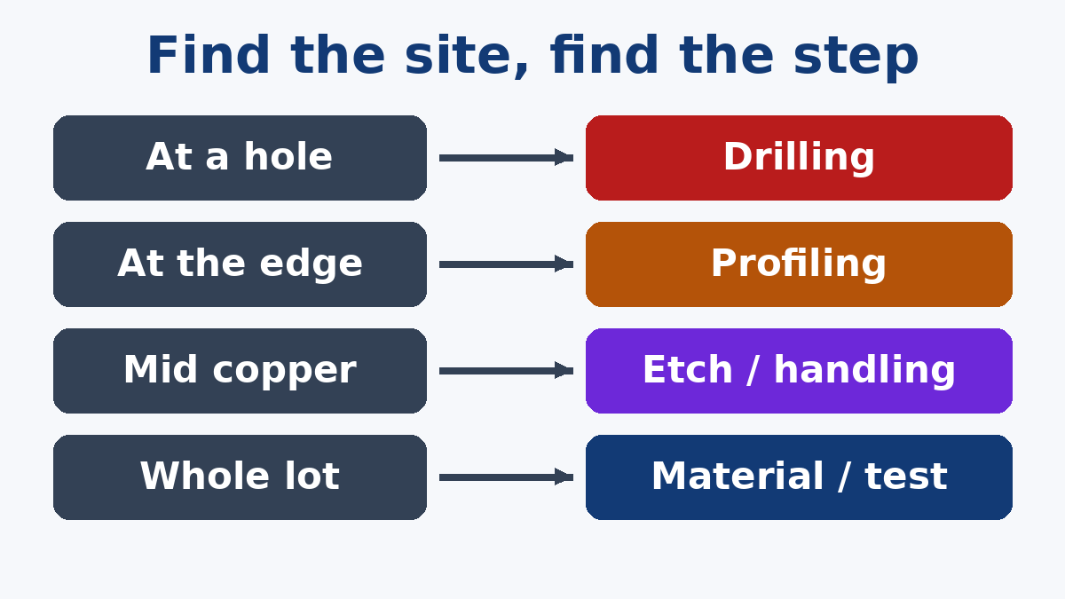
When we analyse a failed board, we section or inspect at the breakdown point rather than guessing, because the site usually points to one of these causes clearly.
Layout choices that make fabrication safer
A few design decisions remove whole categories of risk:
- Keep copper away from the board edge and from score lines, so an edge burr or crack can't reach it.
- Keep copper away from non-plated mounting holes. The wall of a hole drilled through aluminium is bare metal. A screw head or washer that touches a nearby pad connects that pad straight to the base, whatever the dielectric rating. Leave clearance around the hole on the circuit side, or plan insulating hardware.
- Avoid plated through holes in the metal unless the design needs them.
- Allow wider spacing for heavy copper, so etching doesn't have to be pushed.
- Check the depaneling plan. If the panel will be V-scored and snapped at assembly, keep sensitive copper well back from the line, or ask for routed tabs instead.
What to put on the drawing
To make sure the process is controlled against your requirements, not the factory's assumptions:
- Dielectric grade or thermal conductivity, dielectric thickness and base material and thickness.
- Hi-pot conditions: voltage, AC or DC, dwell, leakage limit and sampling.
- Surface finish, with a note if the metal face must be protected from cosmetic damage.
- Cosmetic acceptance for the metal side if it's visible.
- Flatness, if the board mounts to a heat sink.
- Outline method preferences and copper-to-edge clearance.
Our PCB Fabrication Process page describes our general production flow. For metal core work specifically, the Metal Core PCB page is the place to start a quote, and if anything above is missing from your files, we'll ask during DFM review rather than fill it in ourselves.