

Lists of "medical PCB requirements" tend to cover the same ground: comply with ISO 13485, build to IPC Class 3, keep the boards clean, plan for long product life. All true, and we have covered quality systems, traceability and device classes in other guides. But one requirement is written directly into the copper and laminate of many medical boards, and it is the one most often weakened by ordinary manufacturing decisions: the isolation barrier that protects the patient and the operator from mains voltage and from each other.
If a medical device connects to a patient through an applied part, or is powered from mains, its electrical safety evaluation under IEC 60601-1 will look closely at the insulation between circuits. A large share of that insulation is the printed circuit board itself: the gap between copper features on the surface, the air across a slot, and the laminate between layers. A design team can lay that barrier out correctly and still receive boards where it is compromised, because a fab added copper thieving in the gap, substituted a laminate, or shifted an inner layer.
This article looks at the barrier from the factory side: what IEC 60601-1 asks of the board, how fabrication and assembly can erode it, and what to put on the drawing so the barrier you designed is the barrier you get. It is not a substitute for your safety engineer or test laboratory; they set the requirement. Our job, and yours when you write the purchase documents, is to make sure manufacturing preserves it.
What the standard asks of the board
IEC 60601-1 organizes protection against electric shock into means of protection, distinguishing means of operator protection (MOOP) from the more demanding means of patient protection (MOPP). A barrier may need one means of protection or two, depending on what it separates. Each means of protection is achieved with a combination of:
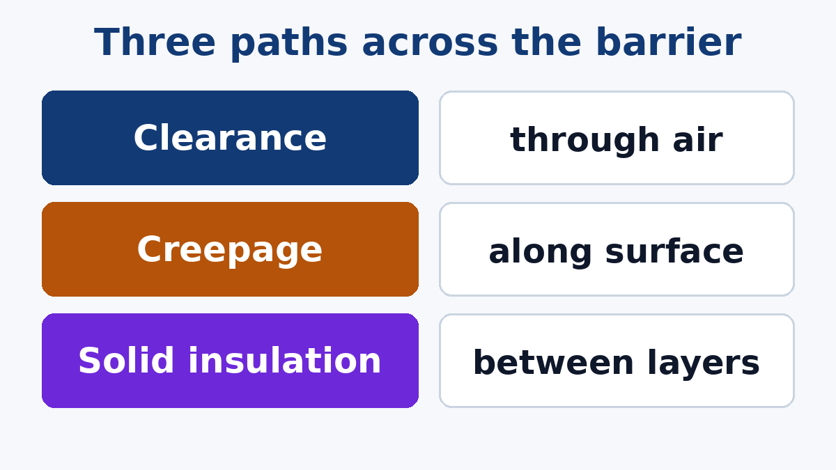
- Clearance: the shortest distance through air between two conductive parts.
- Creepage distance: the shortest distance along the surface of insulating material between them.
- Solid insulation: insulating material, such as the laminate between PCB layers, that must withstand a specified test voltage.
The required values come from tables in the standard and depend on working voltage, the type of protection, and in some cases pollution degree, material group and altitude. As reference points, the commonly cited Table 12 values for patient protection at a working voltage of 250 V rms are 4 mm creepage and 2.5 mm clearance with a 1500 V ac test for one MOPP, and 8 mm creepage and 5 mm clearance with a 4000 V ac test for two MOPP. Those are far larger than the spacing in a normal design-rule file, which is exactly why they are vulnerable: a factory's automated tools see plenty of empty board area to optimize. Take your actual values from the edition and tables your test laboratory applies; operator-protection tables also bring material group (the laminate's comparative tracking index) and pollution degree into the calculation.
The barrier runs through every layer
A barrier is easy to picture on the top layer: a clear band between the primary and the isolated side, perhaps with a routed slot under an optocoupler or transformer. On a multilayer board, the same barrier must hold on every inner layer as well, and the insulation between layers counts too.
Two consequences matter for manufacturing:
Inner-layer copper must respect the gap. A plane or pour on an inner layer that extends into the barrier zone can shorten the distance between hazardous and isolated circuits even when the outer layers look clean. Good practice is to define the barrier as a keep-out on every layer, including planes, and to check the actual Gerber or ODB++ data for each layer, not just the design rules.
Laminate between layers becomes solid insulation. If a hazardous circuit on one layer overlaps an isolated circuit on an adjacent layer, the dielectric between them is the insulation, and the standard places requirements on it: a test voltage, and for some applications a minimum thickness or construction. That makes the dielectric thickness and the material a safety parameter, not just an impedance or cost parameter. A fab that substitutes a thinner prepreg to hit an overall thickness, or a different glass style, has changed your insulation.
How fabrication erodes a barrier
Most of these are ordinary, well-intentioned process steps. They are only harmful because the factory does not know the gap is a safety feature.
Copper thieving and balancing. Fabs often add dummy copper in open areas to even out plating and reduce warpage. An empty isolation band is precisely the kind of area that attracts thieving. Thieving dots inside a barrier reduce creepage and clearance and may be floating conductors that bridge the gap in stages.
Laminate and prepreg substitution. A different laminate may have a different CTI, which can matter where creepage is calculated by material group, and different dielectric thickness or resin content between layers. Substitution is routine in commercial work. For a medical barrier it should require approval.
Registration and etch. Inner-layer misregistration and etch variation move copper edges. The tolerances are small compared with millimetre-scale barriers, so a well-designed barrier has margin, but a design that sits right at the minimum distance has none.
Slot fabrication. Routed slots are used to lengthen creepage paths or force clearance through air. The slot's width, length and position need to be held; a slot that is narrower than designed, or that ends short of the component body it was meant to separate, may not provide the path your calculation assumed. The standard also treats sufficiently narrow grooves as bridged, so slot width matters, not just presence.
Panel features. Breakaway tabs, mouse bites, V-scores, tooling holes and fiducials placed by the panelization engineer can intrude into a barrier at the board edge.
Copper slivers and etch residue. A defect that would be cosmetic elsewhere can be a safety defect in a barrier zone. Bare-board inspection should treat the barrier as a critical area.
How assembly erodes a barrier
The barrier on the bare board can be compromised again on the assembly line:
- Solder balls, splashes and flux residues in or near the barrier zone can bridge part of the distance or form a conductive or hygroscopic path. This is one reason cleanliness requirements matter more on isolation boards.
- Through-hole lead length and clinched leads on the solder side can reduce clearance to the other side of the barrier.
- Component bodies and mounting: a transformer or optocoupler that is not seated flat, or a heat sink or screw near the barrier, changes the geometry the safety evaluation assumed.
- Conformal coating. Where the design relies on coating to justify reduced distances, the coating type, thickness and coverage become part of the barrier and must be controlled, inspected and kept free of voids. Where the design does not rely on it, coating is a bonus, not a substitute for the distances.
- Rework near the barrier can leave residue or damage the surface; it should be recorded and re-inspected.
What to put on the fab drawing and purchase order
The fix for nearly every item above is information. The factory cannot protect a barrier it does not know exists. On the drawing:
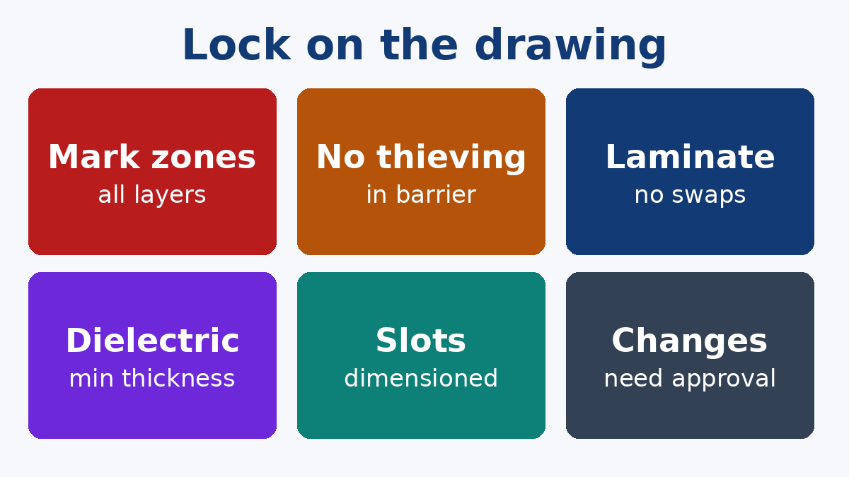
- Mark the barrier. Show the isolation zones on a mechanical layer or the drawing, state that they are safety-critical, and state that no copper, thieving or vias may be added within them on any layer.
- Prohibit thieving and copper balancing in barrier zones explicitly. "No copper may be added in areas marked X" is clearer than a general note.
- Lock the material. Name the laminate and prepreg, or the IPC-4101 specification sheet plus any minimum CTI, and state that substitution requires written approval.
- Lock the dielectric between layers wherever it forms solid insulation: minimum thickness, construction if required, and no change without approval.
- Dimension the slots with tolerances, and state they are part of the isolation design.
- Keep panel features out of barrier zones, or specify the panel yourself.
- Define inspection. Ask for barrier zones to be treated as critical areas in bare-board inspection, and, where justified, for a cross-section to confirm dielectric thickness on a sample or coupon.
On the assembly side, state the workmanship class (IPC-A-610 Class 3 is common for medical but not automatic), the cleanliness requirement and how it will be verified, any coating requirement that the barrier relies on, and whether a production dielectric strength test at board level is expected. If it is, specify the test voltage, duration, current limit and which nets are tied together, and agree a fixture; a hi-pot test is only meaningful if it stresses the barrier you care about.
Changes are the long-term risk
Medical products stay in production for years, and the safety evaluation is tied to the design as tested. Over that lifetime, laminates are discontinued, fabs update processes, assemblers change coatings and fluxes, and components go obsolete. Any of these can touch the barrier.
The practical defence is a change-notification clause: the supplier must notify you, and obtain approval, before changing laminate, prepreg, stackup, solder mask, surface finish, coating, flux or cleaning process, or the manufacturing site for your boards. It costs nothing to write and gives your regulatory team the chance to decide whether a change needs re-evaluation before it is in shipped product.
A factory's view
When we receive a medical design with isolation requirements, the most useful thing a customer can send is a drawing that marks the barrier and a short note on which distances are critical. With that, our CAM engineers can keep thieving and panel features away, check every layer for intrusions, confirm the stackup holds the required dielectric, and flag places where the design sits too close to its minimums to tolerate normal process variation. Without it, we will still spot an obvious isolation gap, but we are guessing at intent, and safety is not a place for guesses.
If you would like us to review a design's barrier before release, our PCB Materials and Medical Devices pages explain how we approach material locks and medical builds, and our engineers can return a layer-by-layer check of the barrier zones with the quote.