
"Should this board be Rogers?" is one of the most common questions on wireless product RFQs. The board might be a Bluetooth sensor, a Wi-Fi gateway, a LoRa node or a cellular IoT device, and someone has read that FR-4 is "not suitable above 1 GHz". The comparison tables online reinforce it: FR-4 has higher loss, a less stable dielectric constant and wider tolerance, so a low-loss laminate must be better.
It is better, electrically. Whether it is needed is a different question, and for many sub-6 GHz products the honest answer is no. For others it is yes, but only on one layer. This article looks at the decision the way we see it from the factory side: what the RF part of the board actually needs, what changes in fabrication when you switch, and how to choose between all-FR-4, hybrid and all-low-loss builds. (We use "Rogers" here the way buyers do, as shorthand for the family of hydrocarbon-ceramic and PTFE-based high-frequency laminates, of which there are several makers.)
Why the "FR-4 stops at 1 GHz" rule is too blunt
Two properties drive the decision: loss and dielectric constant control. They matter differently depending on what the RF circuit looks like.
Loss depends on length. FR-4's dissipation factor is much higher than a high-frequency laminate's, and dielectric loss rises with frequency. But the total loss on a trace is loss per unit length times length. On a typical 2.4 GHz product, the RF path from the radio chip to the antenna is short, often a couple of centimetres. The extra loss on FR-4 over that distance is small compared with antenna efficiency, matching and enclosure effects. On a board with long RF runs, a feed network or a large antenna array, it adds up quickly.
Dk control matters for resonant structures. Impedance of a 50 ohm line is fairly tolerant of small Dk changes. Structures that depend on wavelength, such as printed antennas, filters, couplers and resonators, shift in frequency when Dk changes. FR-4's Dk varies between material suppliers, glass styles, resin contents and lots, and it changes with frequency. A printed antenna tuned on one batch of FR-4 can shift on another. High-frequency laminates hold Dk to a much tighter tolerance.
So the question is not "what frequency?" but "how long are the RF paths, and how much do resonant structures on the board depend on the material?"
When FR-4 is usually enough
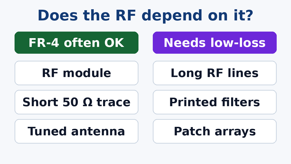
- The radio is a certified module with its own antenna or connector, and the main board only carries digital signals and power to it.
- The radio chip sits close to a chip antenna or connector, with a short 50 ohm trace and a matching network that can be tuned with component values.
- The printed antenna is simple and tolerant, and the design includes a tuning network to absorb material variation.
- Volumes are cost-sensitive and the RF performance target has margin.
In these cases, the useful steps are to specify the FR-4 grade and stackup clearly, control impedance on the RF trace, keep the RF layer's dielectric thickness fixed on the drawing, and check antenna tuning on boards from the production material, not only on prototypes.
When a low-loss laminate earns its cost
- Long RF transmission lines, feed networks or antenna arrays where loss adds up
- Printed filters, couplers or patch antennas whose frequency must not move between lots
- Higher bands within or above sub-6 GHz, where loss and Dk effects grow
- Products with tight link budgets or regulatory power margins
- Phase-matched paths, where Dk variation turns into phase error
What changes in the factory when you switch
This is the part comparison tables rarely cover, and the part that most often surprises buyers.
The stackup follows the material. High-frequency laminates come in a limited set of core thicknesses and copper weights. An FR-4 stackup can be adjusted with different prepreg combinations; a low-loss RF layer usually has to be designed around a thickness the material is actually made in. Design the RF layer on a real, available core first, then build the rest of the stackup around it.
Design Dk is not always the datasheet headline. Many high-frequency laminate makers publish a "design Dk" for modelling, which can differ from the value measured by the specification test method. Use the design value, at your frequency, for impedance and antenna calculations.
Bonding materials matter. Hydrocarbon-ceramic laminates can usually be processed much like FR-4 and bonded with compatible prepregs. PTFE-based laminates need different hole preparation, drilling parameters and bonding materials. In a hybrid, the bonding layer is part of the RF environment for any adjacent stripline.
Material use and minimums. The laminate comes in full sheets and is expensive per unit area. For a small board ordered in small quantities, the cost can be driven by how much of the sheet the panel uses, not by the board area. Hybrid builds use low-loss material only for the RF layer, which helps.
Availability. Common thicknesses of the most widely used high-frequency laminates are often available, but less common thicknesses, copper weights or a specific product name may need to be ordered, which adds time. Allowing an approved equivalent with the same design Dk and loss class gives the fab more options.
Finish and solder mask on RF lines. Solder mask over an RF trace changes its impedance and adds loss; many RF designs leave the RF trace unmasked or define the mask openings carefully. Surface finish on exposed RF copper also affects loss, so the finish choice should be made with the RF layer in mind. Our High Frequency PCB page covers the build options we offer.
Three build options
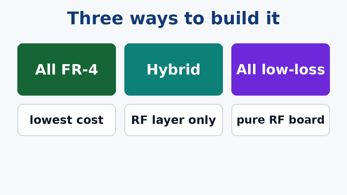
All FR-4. Lowest cost and simplest supply. Suitable when the RF path is short, the antenna tolerant or tuned, and the margin adequate. Specify the FR-4 grade and RF layer thickness, and validate on production material.
Hybrid. A low-loss core forms the RF layer, usually the top layer and its reference plane, with FR-4 for the remaining layers. This is common for multilayer wireless boards that need stable RF structures plus dense digital routing. It adds lamination and drilling considerations (different expansion, resin systems and hole preparation), so agree the construction with the fab before layout.
All low-loss. Usually a two-layer or simple multilayer RF board: antennas, front ends, filters, or a dedicated RF board connected to an FR-4 main board. Highest material cost per area, but simplest construction for pure RF circuits.
Splitting the product into an FR-4 main board and a small low-loss RF board is sometimes cheaper than a large hybrid, because the expensive material is only used where it is needed.
Questions to settle before the RFQ
- Which RF structures are on the board, and how long are the RF paths?
- Is the antenna printed, and does the design include a tuning network?
- Which layer carries RF, and what is its reference plane?
- Which core thickness, copper weight and design Dk is the RF layer designed on?
- Is an equivalent material acceptable? If so, which properties define "equivalent"?
- What impedance tolerance is required on the RF trace, and how will it be verified?
- Will solder mask be removed from the RF traces?
If you send us the stackup idea and the RF requirements, our engineers will tell you which build we would recommend, which materials we can source in the thickness you need, and how the choice affects cost and lead time. For RF traces that need controlled impedance on any material, see our Impedance Control PCB service.