

A familiar story in high-speed hardware: the prototype boards work. Eye diagrams look healthy, the link trains, the product ships. Then a later production lot, or the first lot from a second supplier, starts showing link errors, retraining, or failures at temperature, and nobody changed the design.
Usually something did change, just not in the Gerbers. Signal integrity depends on physical properties of the finished board: dielectric thickness, conductor width and shape, the glass under a trace, how much copper was plated on an outer layer, what a via looks like after drilling. Each of those varies from lot to lot and from fab to fab within a tolerance. A design that was tuned to one set of values, with little margin, can drift out of spec when those values move.
This article looks at signal integrity from that angle: the classic SI problems of reflections, crosstalk, return paths and skew, and specifically how manufacturing variation feeds each of them. It is written from our CAM and fabrication floor in Shenzhen, where we see both the design intent and what the process can realistically hold. Channel loss budgets, material loss and copper roughness are a closely related topic that we treat separately; here the focus is on keeping signals clean and on margin against real-world variation.
The problems, briefly
Signal integrity problems in digital boards fall into a few families:
- Reflections from impedance discontinuities: a change in trace width, a via, a connector, a stub, a gap in the reference plane. Part of the signal bounces back, distorting edges and closing the eye.
- Crosstalk between neighboring conductors, coupled through electric and magnetic fields. It grows with parallel length and with closer spacing, and shrinks the closer a trace is to its reference plane.
- Return path problems: every signal current has a return current flowing in the nearest reference plane. If that plane is split, voided or changes between layers without a nearby return via, the loop grows, inductance rises, and the signal couples into everything around it.
- Timing and skew: delay mismatch within a differential pair or across a parallel bus.
- Power noise coupling into signals, which is a power integrity topic in its own right.
Each of these has a design answer. What gets less attention is how each depends on things the fab controls within a tolerance.

Impedance: a target with a tolerance, not a number
Characteristic impedance depends on trace width and thickness, dielectric thickness to the reference plane(s), and the dielectric constant of the material around the trace. Every one of those varies:
- Trace width varies with etching. The cross-section of an etched trace is a trapezoid, not a rectangle, and the top width differs from the bottom. Outer-layer traces also get plated copper, which changes both thickness and shape.
- Dielectric thickness depends on the prepreg's resin content and how much it flows during lamination, which in turn depends on the copper density of adjacent layers. A prepreg between two dense planes ends up thinner than the same prepreg next to sparse routing.
- Dielectric constant varies with resin content and glass style, and with frequency. The datasheet value for a laminate is often a single number, but the value that matters is the one for your specific construction at your frequency.
- Solder mask over outer-layer traces lowers their impedance slightly, and its thickness varies.
This is why a controlled-impedance design should specify a target and a tolerance, and allow the fab to adjust trace width within limits to hit the target with its actual materials and process. A fab that builds impedance control PCB work routinely will model the stackup, adjust widths, build test coupons on the production panel and measure them by TDR. The design side of the bargain is to leave room: a design that only works at exactly 100 ohms differential has no margin for a normal process tolerance.
Reflections that come from the process
Some discontinuities are drawn in the design. Others appear in manufacturing:
- Via stubs. A through via used to change from a top layer to an upper inner layer leaves an unused barrel below. That stub resonates and reflects. Its length depends on board thickness, so a small thickness variation shifts the resonance. Back-drilling removes most of the stub, but leaves a small residual length that depends on depth control. Specify which vias must be back-drilled and the maximum residual stub you can accept, and let the fab tell you what it can hold.
- Antipad and via geometry. The clearance around a via in each plane sets part of the via's impedance. Drill registration and hole size tolerance move it slightly.
- Pad and connector transitions. Large pads for connectors or AC coupling capacitors are capacitive discontinuities. Plane cutouts under those pads are a common fix, and they need to be in the data, not assumed.
- Neck-downs. Where a trace narrows to escape a BGA, its impedance rises. The escape is short enough to be tolerable in most designs, but etch variation affects narrow traces proportionally more.
Crosstalk depends on dielectric thickness
Crosstalk is primarily set by spacing between traces and the height of the traces above their reference plane. Both are layout choices, but the height is really a dielectric thickness, and that is a fabrication variable. A stackup that was optimized to squeeze traces close together at a particular dielectric thickness can see noticeably more crosstalk if the dielectric comes out thicker.
Design with margin on spacing for long parallel runs, keep aggressive high-speed routing close to a solid reference, and if a different fab will build the board, check that its proposed stackup keeps those heights.
Return paths: the plane has to actually be there
Return path problems are mostly design issues, but manufacturing affects them in two ways.
First, plane voids from antipads. A dense field of vias, as under a large BGA or a connector, removes a lot of copper from each plane. If antipads merge, the plane under a trace running through that field can be much less solid than the designer imagined. Check the plane layers in the actual Gerbers, not just the routing layers.
Second, thieving and copper balancing. Fabs sometimes add copper in open areas to balance plating or reduce warpage. Floating copper near high-speed traces can create resonances and coupling. Mark areas where thieving is not allowed, and state whether it must be grounded if used.
When a signal changes layers, its return current needs a path between the corresponding reference planes. Place return (stitching) vias near signal vias that change reference, particularly when the reference changes between different nets.
Skew: the glass under the trace
Laminate is made of woven glass cloth impregnated with resin. Glass and resin have different dielectric constants, so a trace running along a glass bundle sees a slightly different effective dielectric constant from one running over a resin-rich gap. For a differential pair, if one conductor sits over glass and the other over resin for a long distance, the two see different delays: skew that converts some of the differential signal into common mode.
This effect is lot-dependent because exactly where the weave falls relative to your traces varies from panel to panel. Mitigations include spread or more uniform glass styles, routing at a small angle to the weave, rotating the design on the panel, or zig-zag routing on long pairs. Some of these cost panel utilization, so discuss them with the fab rather than just writing "rotate 10 degrees" on the drawing.
Why the second fab's boards behave differently
When a design moves to a new supplier, the most common SI surprises come from:
- A different laminate that meets the same generic description but has different dielectric constant, glass style or resin content.
- A different stackup built to hit the same overall thickness with different prepregs.
- Different etch compensation, giving a different trace shape at the same nominal width.
- Different copper foil, which affects loss and slightly affects impedance.
- A different surface finish or solder mask thickness on outer-layer microstrips.
None of these is wrong. They are why your data package should specify performance (impedance with tolerance, material by IPC-4101 slash sheet or approved product, maximum residual stub, dielectric thickness where it matters for crosstalk) instead of relying on the first fab's defaults. Our PCB Materials page is a starting point for the material conversation.
Design for margin, then verify
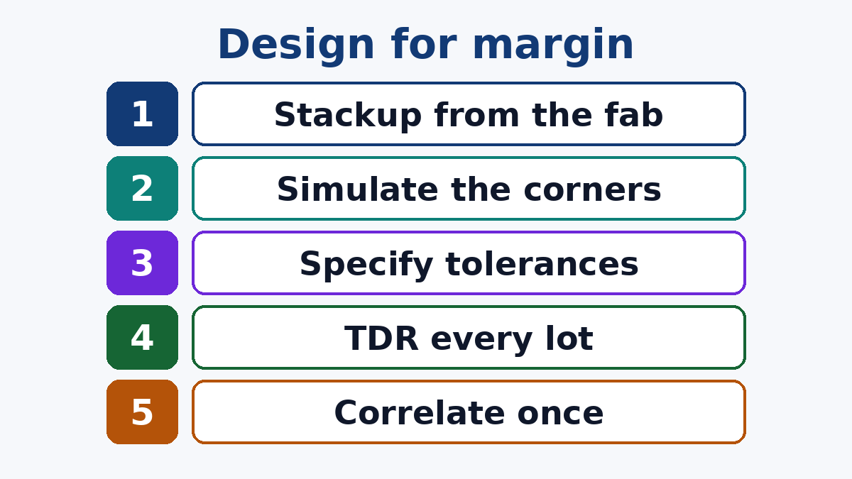
A practical approach that holds up across lots and suppliers:
- Agree the stackup with the fab before routing. Get the modeled dielectric thicknesses and trace geometries from the fab that will build it, not from a generic calculator.
- Simulate the corners. Run SI simulation at the nominal stackup and at the tolerance extremes of dielectric thickness, trace width and dielectric constant. If the design fails at a corner, it will fail on some lot.
- Specify what matters. Impedance targets and tolerances by layer and structure, reference planes, back-drill requirements, thieving keep-outs, material requirements.
- Require evidence per lot. TDR coupon results on every production panel or lot for impedance-controlled boards. Cross-sections when stackup accuracy is critical.
- Correlate once. Measure a few production boards against your simulation and your prototype to confirm the model reflects reality. When a new supplier comes in, repeat that correlation.
A short checklist for the fab drawing
- Impedance table: layer, structure (single-ended, differential, coplanar), target, tolerance, reference layers.
- Permission to adjust trace widths within a stated range to meet impedance.
- Material by IPC-4101 slash sheet or approved product list; note if glass style matters.
- Back-drill layers, from which side, and maximum residual stub.
- Areas where copper thieving is prohibited.
- TDR coupon testing requirement and report per lot.
Signal integrity problems that appear only in production are rarely mysterious once the manufacturing variables are on the table. If you are preparing a high-speed design, send us the stackup and impedance requirements before routing is final; our CAM engineers will model it with the materials we would actually use and tell you where the margin is thin.