
Buyers and engineers type “what is an HDI PCB” when a BGA pitch, board outline, or layer count starts fighting conventional through-hole multilayer. The useful answer is not a brochure claim that HDI is simply “better.” It is a density definition, a microvia role, a short map of stacked versus staggered interconnect, a gate for when HDI beats conventional multilayer, and the China fab process steps and RFQ fields that make quotes comparable.
This primer stays at buyer and engineer level. It does not replace a stackup and DFM selection gate, a manufacturing capability menu, a PDN or impedance deep dive, or an aerospace process-system page. Those jobs need their own drawings and travelers. Here the goal is shared language: what HDI means on a fab note, what laser microvias buy you, and what to name before a China shop invents a quieter build.
What “HDI” means in factory language
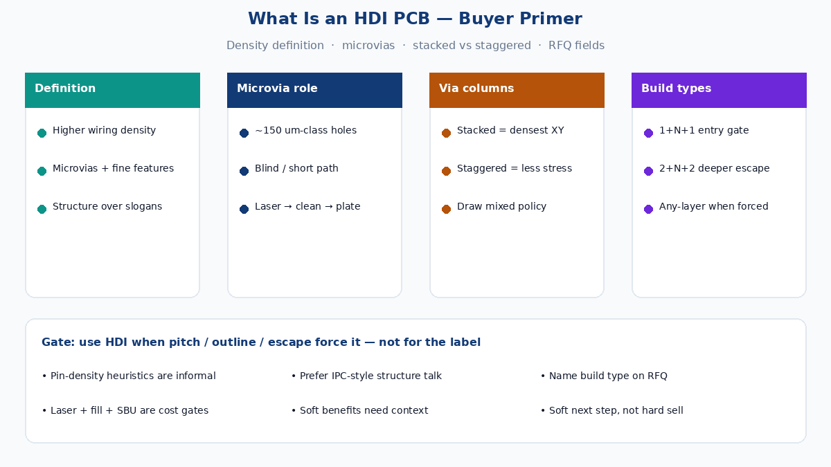
HDI stands for high-density interconnect. In plain fab speech, an HDI PCB is a board whose wiring density per unit area is high enough that conventional plated through-holes (PTH) alone cannot escape pads, meet outline, or keep layer count honest. The industry reaches that density with finer lines and spaces, denser connection pads, and — most characteristically — laser-drilled microvias that connect only a few layers at a time instead of drilling through the whole stack.
Standards language (IPC-2226 style) talks about HDI structures by how microvias and cores are arranged — single-level build-ups, multi-level build-ups, buried vias, and any-layer constructions — not by a single pin-count slogan. Some market primers cite rough pin-density heuristics such as “about 120–160 pins per square inch.” Treat those as informal industry talk, not a hard IPC pass/fail number you can put on a drawing. What CAM and procurement actually share is structure: microvia presence, build-up count, and whether vias are blind, buried, stacked, or staggered.
Three traits show up on almost every real HDI traveler:
Higher wiring density per area. More nets and pads in less XY space — often forced by fine-pitch BGA / CSP packages and frozen outlines.
Microvias as the normal interconnect. Holes with diameters typically discussed at 150 µm or less (plant finished diameter varies), laser-drilled into dielectric to a capture pad, then plated.
Sequential build-up (SBU). Outer HDI layers are laminated, laser-drilled, and plated in cycles rather than one full-thickness drill of every hole.
Calling a board “HDI” because the soldermask looks fine or because marketing wants the word is how quotes diverge. The fab prices laser stations, fill, and extra presses — not the adjective.
Microvias: the feature that makes HDI work
A microvia is a small blind (or sometimes buried) via that connects adjacent or near-adjacent layers. Unlike a PTH that punches the entire board thickness, a microvia stops on a capture pad a dielectric thickness away. That short path is what lets designers put vias in or near fine pads, free routing channels, and cut the need for dogbones that eat BGA escape space.
Diameter and depth. Industry discussion often puts microvia diameters at roughly 150 µm or below; many mainstream builds sit in a tighter finished band once the plant names its laser and dielectric. Depth is set by the buildup dielectric thickness. Aspect ratio — depth divided by diameter — matters because plating must wet and fill the wall without voids. Deep, skinny holes starve copper; shallow, well-proportioned holes plate cleaner. Confirm aspect with the cited fab and stackup — do not paste a brochure ratio as a promise.
Laser drill, clean, plate. Typical flow: laminate laser-drillable dielectric (prepreg or RCC class materials the plant stocks), laser-open the via, desmear or clean residue, metallize and plate the wall, then fill and planarize when via-in-pad or stacked columns need a flat copper land for the next laser or for SMT paste. Laser Direct Imaging (LDI) often rides alongside fine-line outer layers because film contact imaging struggles at HDI feature sizes — but LDI alone does not make a board HDI.
Blind and buried. Blind vias connect an outer layer to an inner layer without going through. Buried vias sit entirely inside the stack. Microvias are the common blind tool on HDI skins; buried structures still appear in cores and multi-level builds. Name which nets need which via type on the fab note so CAM does not substitute PTH dogbones where density dies.
Without microvias, “HDI density” collapses back to finer etch on a through-hole multilayer — useful sometimes, but not the same process or price family.
Stacked vs staggered microvias (primer)
Once you have more than one buildup level, microvias can sit on top of each other or offset.
Stacked. Successive microvias share the same XY center. The lower via is usually filled and copper-capped so the next laser lands on copper. Stacked columns buy the tightest vertical interconnect in the smallest footprint — and add fill, planarization, and plating interfaces that thermal cycling will stress. Prefer stacked only where escape leaves no room to offset and the plant has proven fill/cap for your copper and dielectric.
Staggered. Each microvia lands on a capture pad offset from the via below. You spend a little pad real estate; you often gain simpler plating and a friendlier reliability discussion because stress is not concentrated in one filled column. Prefer staggered when a few mils of offset exist and life or multi-reflow arguments matter more than absolute density.
Mixed policies are normal: stagger where you can, stack only under the BGA escape that forces it. Draw the policy. A one-line “stacked HDI” on the RFQ is how a whole board inherits the harder process.
This primer stops at that buyer gate. Plating stress maps, coupon strategies, and confirm-with-fab DFM bands belong on a dedicated stackup and DFM page — not repeated here as if one article owned every µm.
Build-up types buyers should recognize: 1+N+1 vs any-layer
Fab travelers speak in build notations. You do not need an encyclopedia of every IPC type chart to RFQ, but you do need the three phrases shops price differently:
1+N+1. One HDI buildup layer on each side of a multilayer core N. Entry HDI for many fine-pitch escapes: one microvia level per face, laser + one extra press cycle family per side.
2+N+2. Two sequential buildups each side of core N. Deeper escape, more laser and lamination cycles, more registration exposure.
Any-layer (often called ELIC in buyer decks). Laser microvias available across nearly every layer pair — highest density and cost class. Not “better 2+N+2”; a different process family. Buy it when density math leaves no staggered or single-level path, not because a datasheet used the word.
Writing “8-layer HDI” without 1+N+1 / 2+N+2 / any-layer lets the plant quote a single laser skin or a full any-layer stack. Put the notation on the stackup drawing, fab note, and PO the same way. Loose mapping to IPC-2226-style structure ideas is fine for internal education; the PO needs the build string the traveler will run.
When HDI beats conventional multilayer — and when it does not
Start with geometry and cost of alternatives, not prestige.
HDI starts earning money when:
- BGA / CSP pitch and pad count choke PTH dogbone escape.
- Board outline is frozen and density must come from via architecture, not extra XY.
- Adding two or four conventional layers still cannot escape or meet impedance / thermal notes without shrinking features past PTH capability.
- Via-in-pad under fine balls is required and open PTH under the pad is not an assembly plan.
Conventional multilayer often still wins when:
- Coarse pitch and ample board area leave room for PTH fan-out.
- A slightly larger outline or two more PTH layers is cheaper than a laser buildup cycle.
- The design is mostly digital with modest density and no frozen smartphone-class outline.
- Schedule and yield risk of sequential lamination outweigh the density gain.
A practical test: if CAM can escape with through-hole multilayer at acceptable size and layer count, skip HDI for the label. If CAM already flags annular-ring starvation, dogbone collisions, or “cannot escape without blind vias,” name a build type — not “HDI capable” as a slogan.
Soft claims you will see in generic primers — “always cheaper materials,” “always faster prototypes,” “inherently higher heat resistance” — need context. Smaller boards can use less laminate, but laser, fill, and multi-lam add cost and scrap risk. Proto lead time depends on the shop’s HDI line load, not the acronym. Thermal behavior depends on copper, dielectric, and stack — HDI is not a heatsink by definition. Keep benefits tied to density, path length, and layer-count tradeoffs you can draw.
China fab process gates: laser, fill, sequential lamination
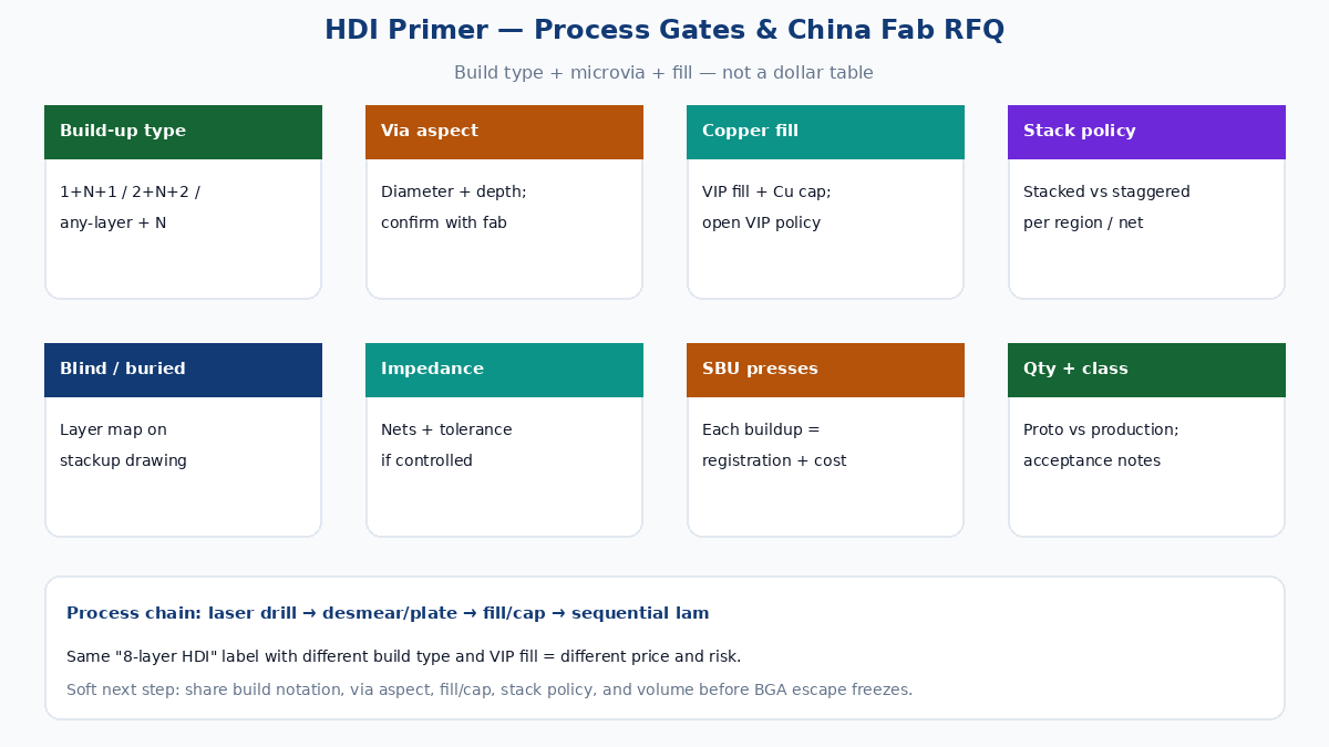
Overseas buyers who only write “HDI, quick turn” inherit house defaults. The gates that actually move price and yield are process steps:
1. Laser drill for microvias. CO₂, UV, or hybrid lasers — plant-owned choice. Dielectric must be laser-drillable at your diameter. Standard FR-4 is not automatically friendly at every feature size; ask for the buildup material family the shop stocks.
2. Desmear / clean and plate. Residue after laser kills wetting. Plate builds wall copper; starved knees and thin barrels show up in microsections after reflow even when electrical test beeped green.
3. Via fill and copper cap. Resin or conductive fill plus planar copper cap (VIPPO-style language) when vias sit in SMT pads or when stacked lasers need a copper land. Open via-in-pad under fine-pitch BGA invites wicking and voids — treat fill/cap as a named RFQ line, not an assumed habit.
4. Blind and buried via planning. Which layers connect where drives drill and lam sequence. Vague “blind OK” without a stackup invites wrong depths.
5. Stacked and staggered policy. Documented per region or net so CAM does not stack every column.
6. Sequential lamination (SBU). Each extra buildup is another press, another registration chance to eat annular ring, and another schedule step. Cost and scrap rise non-linearly — 2+N+2 is not “twice 1+N+1” on the calendar.
7. LDI and fine-line etch. Often paired with HDI outer layers. Call critical trace/space and copper weight so etch capability is confirmed, not assumed from a marketing µm number.
These gates are why two “HDI” quotes can differ by multiples: one shop quoted a 1+N+1 with filled VIP; another quoted a cosmetic laser dogbone on a through-hole core. Normalize the traveler before you compare unit price.
RFQ fields that keep HDI quotes honest
Weak RFQs say “HDI PCB, 8 layer, ENIG.” Strong RFQs name structure and acceptance so CAM cannot invent a quieter stack.
| Field | Why the shop needs it |
|---|---|
| Build-up type | 1+N+1 / 2+N+2 / any-layer with N defined on the stackup |
| Layer count and stackup | Core vs buildup dielectrics, copper weights outer / buildup / core |
| Microvia diameter and aspect | Finished or drilled intent + dielectric thickness; confirm aspect with fab |
| Stacked vs staggered | Policy per region or net; mixed allowed if drawn |
| Blind / buried map | Which layers connect; no “blind OK” without a drawing |
| Via fill / copper cap | Resin or conductive fill + planar Cu cap where via-in-pad; open VIP policy |
| Impedance | Controlled nets, stackup reference, tolerance — if any |
| Materials notes | Laser-drillable buildup family, Tg / thermal notes for multi-lam and reflow |
| IPC class / acceptance | Product class on the fab note; coupon or microsection expectations when density is high |
| Quantity and revision | Proto vs production band; frozen Gerber / stack revision |
| No silent downgrade | No build-type, VIP, or class cut without signed EQ |
Impedance and PDN plane details deserve their own models and pages; here they appear as RFQ locks so the quote includes the right stack, not as a full signal-integrity course. Do not invent dollar tables or certificate claims on the cover sheet. Ask for process capability that matches the drawing you will freeze.
Soft next step
An HDI PCB is a high-density interconnect board: more wiring per area than conventional PTH multilayer, built with microvias, fine features, and usually sequential build-up. Microvias at roughly 150 µm-class diameters (confirm finished size with the plant) carry the density; stacked versus staggered chooses footprint versus process stress; 1+N+1 versus 2+N+2 versus any-layer chooses how many laser and press cycles you buy. Use HDI when pitch, outline, or escape force it; stay on conventional multilayer when a little more area or a few more PTH layers still closes the design. On China fab RFQs, name build-up type, via aspect, copper fill / cap, stacked policy, and impedance intent so quotes describe the same traveler. Share that package with manufacturing engineering before BGA escape freezes — the right HDI choice is a structure and process contract, not a marketing adjective.