
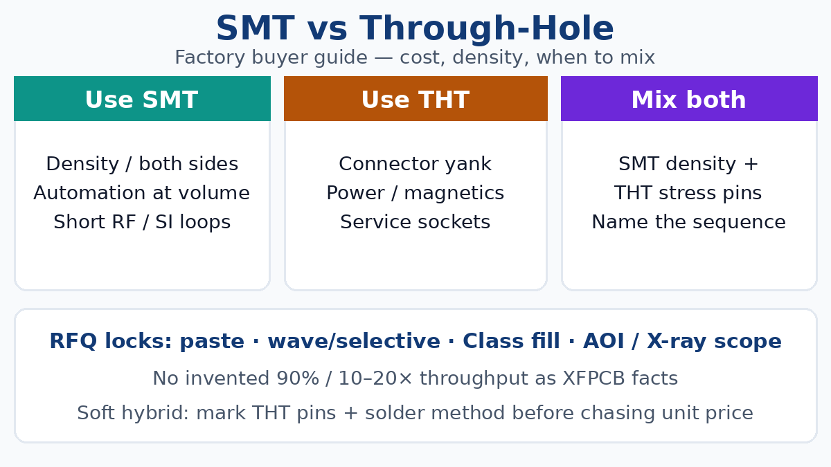
SMT puts parts on copper pads and solders them in a reflow oven. Through-hole (THT / PTH) pushes leads through plated holes and solders the other side — by wave, selective, or hand. Most production boards today are mixed: dense SMT for ICs and passives, through-hole where connectors take cable yank, power pins carry current, or field service still needs a socket. Brochure “showdowns” crown SMT on cost, space, and speed, then nod that THT survives for connectors, power, and hobby. Factory buyers quoting China PCBA need more than that scoreboard. This guide covers when to stay SMT-only, when THT is required, how mixed-technology order of operations actually runs on a traveler, which RFQ fields keep paste / wave / selective / Class fill / inspection comparable, and DFM notes for SMT pads versus through-hole lands — without inventing placement-rate percentages, “10–20×” throughput claims, or XFPCB unit prices.
What SMT and through-hole mean on a China traveler
On the floor, the labels map to process steps, not marketing eras.
| Term | Factory meaning | Buyer trap |
|---|---|---|
| SMT / SMD | Paste print → pick-and-place → reflow on surface pads | Treating “we have SMT” as proof they can run your finest pitch and double-sided recipe |
| Through-hole / THT / PTH | Leads insert through plated holes; solder by wave, selective, or hand | Using “DIP” as if every THT part were a dual-in-line IC |
| Mixed technology | SMT plus THT on one assembly (typical modern PCBA) | Quoting SMT-only unit rates against a BOM that still has connectors and power terminals |
| Selective / wave / hand | How the THT joints get made after (or around) SMT | Leaving the method blank so two plants price different tooling and labor against the same Gerber |
“DIP assembly” in many China RFQs is slang for through-hole capacity — headers, transformers, relays, terminals — not only DIP ICs. Write THT / PTH insertion + solder method on the RFQ. Keep “DIP” for the package when that is what you mean.
This page is a factory buyer decision guide. It is not an IoT product build guide (sense / compute / radio / power domains belong on a different traveler) and not a package glossary that stops at DIP vs SMD naming.
When SMT is the right default
Choose SMT-first when density, automation, and short lead parasitics matter more than pin yank strength.
Prefer SMT when:
- The BOM is mostly chip resistors, capacitors, QFN / BGA / fine-pitch ICs, and connectors available in surface-mount form
- Both sides of the board need parts (through-hole consumes the vertical column of every drilled hole)
- High-volume or mid-volume runs where pick-and-place + reflow amortizes stencil and feeder setup
- Signal integrity and RF front-ends need short loops — long THT leads are stubs you did not design
- Weight and outline are constrained (wearables, modules, dense industrial controllers)
Cost at scale usually favors SMT because paste, place, and reflow are machine-paced. That does not mean every prototype is cheaper as SMT: stencil fabrication, machine programming, and feeder setup still land as NRE. For a ten-board spin with mostly through-hole odd-forms already on the bench, hand-insert THT can still be the lower total path. Write the volume and NRE assumptions on the RFQ so plants do not silently bake high-volume SMT overhead into a proto quote — or the reverse.
Space and routing follow the same logic: no component drill frees inner-layer channels and allows dual-sided placement. Brochure density ratios vary by package mix; treat them as orientation, not XFPCB capacity claims. Ask the fab for your panel density and side constraints instead of pasting industry averages into the SOW.
When through-hole still wins
THT is not obsolete. It is the answer when the failure mode is mechanical or current, not millimetres of real estate.
Prefer THT / PTH when:
- Connectors face repeated mating, cable side-load, or panel mount loads that would lift SMT pads
- Power pins, heavy magnetics, or fuse holders need copper cross-section and hole thermal mass that a small SMT pad cannot match without heroic copper and via arrays
- Vibration / shock duty needs leads anchored through the board (often with staking or conformal coat called out separately)
- Field service still expects sockets, replaceable relays, or hand-solderable modules
- Parts are only available in through-hole (some transformers, high-voltage parts, legacy industrial connectors)
- Very low volume where stencil + SMT programming NRE dominates and the BOM is THT-heavy
Hobby and lab boards often stay THT because parts are large, visible, and reworkable with an iron. That is a valid use case — it is not the same traveler as a Class 3 industrial mixed-tech build. Name the duty and IPC class so the plant does not apply hobby fill rules to a safety-critical product.
When mixed technology is the real answer
Most China PCBA quotes that look “SMT” still ship with a handful of through-hole connectors or power parts. Mixed-tech is the default modern assembly, not a special exemption.
Mixed-tech design rules of thumb:
- Keep THT parts to the minimum set that stress or current forces — every extra pin is an insert + solder cycle
- Place THT so wave or selective nozzles can reach without shadowing tall SMT cans and connectors already reflowed
- Decide early whether THT sits on one side only, and whether any SMT lives on the wave side (palleting / glue / selective becomes mandatory language)
- Lock press-fit vs soldered connectors in writing — press-fit is not “THT wave” on the traveler
A soft hybrid CTA for buyers: send the BOM with package and mounting type columns filled, plus a one-line process intent (“SMT both sides → selective THT topside connectors”). Plants quote faster when they are not inventing your sequence.
Mixed-technology order of operations (what to write on the RFQ)
Brochure articles rarely spell the sequence. China assembly houses do. A typical mixed board runs something like:
- Solder-paste print through a laser-cut (or electroformed) stencil onto SMT pads
- Pick-and-place SMT components (possibly both sides: bottom glue or dual reflow recipe as agreed)
- Reflow SMT joints; SPI / AOI gates as specified
- THT insertion (manual, semi-auto, or axial/radial machinery for odd-forms)
- Wave, selective, or hand solder for through-hole joints
- Touch-up / cleaning if required by residue class
- Final AOI / X-ray / ICT / FCT per the PO — not “100% inspected” with no method
Variants exist: selective first for tall parts, pin-in-paste (THR) where through-hole pins reflow with SMT paste, or pure wave on single-sided boards with no fine-pitch SMT on the wave side. Do not leave the sequence blank. Two bidders pricing different orders against the same Gerber will not be comparable, and the cheaper one often omitted selective tooling or assumed hand solder on fifty pins.
Pin-in-paste / through-hole reflow deserves an explicit yes/no. If you want it, call out paste volume, hole size, and which pins participate. If you do not, say “no THR — wave or selective after reflow” so CAM does not invent a hybrid that your thermal profile cannot survive.
Paste stencil, wave, and selective — RFQ questions that change price
Paste / stencil
- Stencil thickness and aperture reduction rules for fine-pitch vs large power pads
- Step-stencil or nano-coat needs for mixed paste volumes on one panel
- Who owns the stencil (customer vs plant), storage, and revision control when pads change
- SPI (solder paste inspection) sampling or 100% — silent SPI is often “none”
Wave vs selective vs hand
- Wave: high throughput for many THT pins on a pallet-friendly layout; risk of bridging and SMT shadowing if SMT sits on the wave side without glue or masking
- Selective: programmed nozzles for connectors and sparse THT after SMT; tooling and program NRE, better control near fine-pitch zones
- Hand: low pin count, rework, or geometries selective cannot reach; labor-heavy at volume
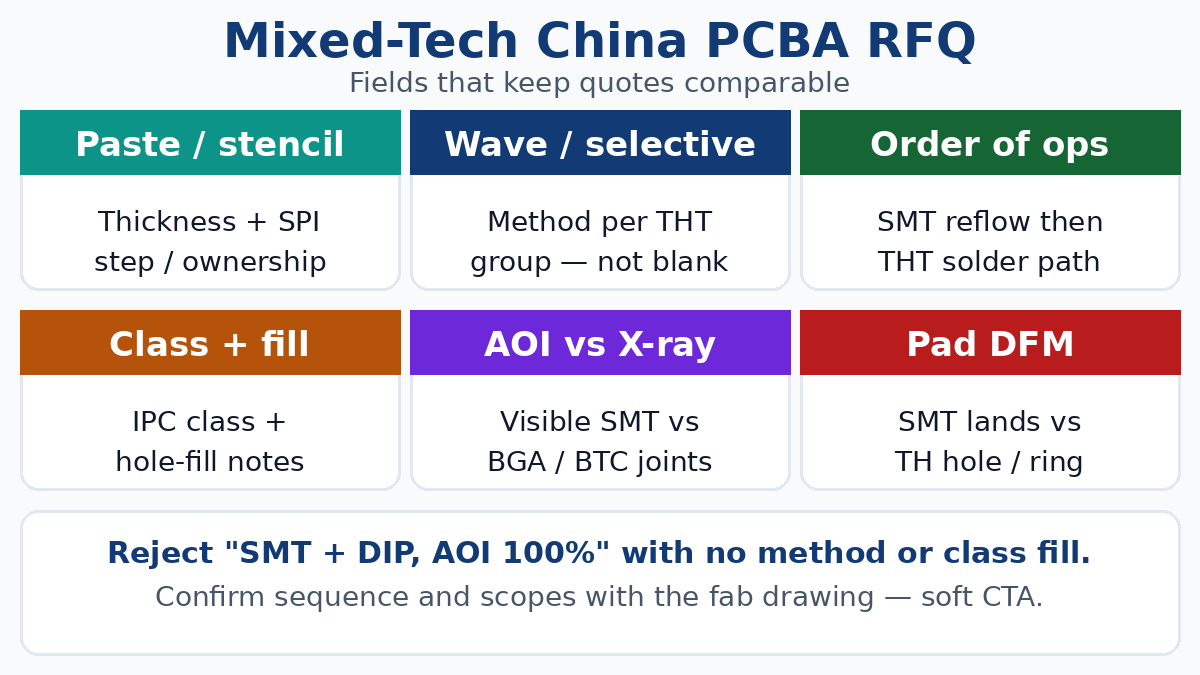
Ask each bidder to name the method per THT reference designator group, not a single checkbox “through-hole: yes.” That one line separates a real process quote from a hopeful average.
IPC Class and hole fill — say it out loud
“Class 2” or “Class 3” on the PO is not decoration. Through-hole vertical fill, wetting, and void expectations change with class and with whether the joint is supported / unsupported. If the drawing is silent, plants default to house Class 2 cosmetics and fill that may fail your acceptance later.
Buyer language that travels:
- IPC class for assembly (and fab, if separate)
- Hole-fill acceptance reference (drawing note or class default) for plated through-hole solder joints
- Whether bottom-side fillets must be visible on specific connectors
- Lead tinning / flux type constraints when cleaning is limited
Do not invent a numeric fill percentage as an XFPCB house claim. Point at the class and the drawing; confirm with the fab on first article.
AOI vs X-ray for BGA (and what THT inspection does not cover)
AOI after reflow catches polarity, missing parts, shifts, and many bridges on visible SMT. It does not see joints under a BGA, CSP, or QFN thermal pad. X-ray (2D / 2.5D / CT as scoped) is the tool for hidden solder: void percentage criteria, open balls, head-in-pillow suspicion — whatever your quality plan names.
Through-hole wave or selective joints are mostly visible or partially visible; AOI or human visual may suffice for pin presence and fillet shape, but that does not replace X-ray for the BGA two centimetres away. Mixed-tech boards need both scopes written down:
- AOI recipe coverage (sides, which packages)
- X-ray sampling or 100% for named BTCs / BGAs
- Separate visual / AOI plan for THT connectors after wave or selective
A quote that only says “AOI + X-ray included” without package lists is not a comparable inspection quote.
DFM notes: SMT pads vs through-hole lands
Small DFM misses are how mixed boards fail at CAM or at first wave.
SMT pad DFM (buyer asks)
- Pad geometry matches the land pattern library the plant actually runs (IPC-compliant vs house shrink)
- Solder-mask defined vs copper-defined pads called out for fine pitch
- Paste aperture vs pad ratio reviewed for QFN centers and large exposed pads
- Keepouts for tall parts that block nozzle or wave access later
Through-hole DFM (buyer asks)
- Finished hole size vs lead diameter (too tight → insert damage; too loose → weak fill and float)
- Annular ring and tear-out risk on connectors under mechanical load
- Thermal relief vs solid spoke on power pins — solid pours that look good in CAD can starve wave heat
- Orientation and clinch rules if clinching is allowed
- Edge clearance so selective nozzles and pallets do not collide with the outline
Send a short DFM questionnaire with the RFQ: “Confirm hole-to-lead for J1–J4; confirm no SMT within ___ mm of wave side for U-can; confirm stencil step need for QFN + large inductor.” Written answers beat a generic “DFM OK” stamp.
China PCBA RFQ checklist (comparable quotes)
Use this as a paste block; adjust to your drawing.
- Mounting type column on the BOM (SMT / THT / press-fit / mechanical)
- Process intent: SMT sides + reflow count; then wave / selective / hand / THR for each THT group
- Stencil ownership, thickness intent, SPI yes/no
- IPC class + hole-fill / fillet notes for THT
- AOI scope; X-ray scope for named BGAs / QFNs
- Odd-form list (transformers, tall electrolytics, shielded cans) and who inserts them
- Panelization / depanel method near heavy connectors
- First-article hold criteria before volume (FAI language separate from FQC cosmetics)
- Cleaning / residue class and conformal coat sequence if coat is required
- Soft ask: confirm-with-fab any pin-in-paste or selective nozzle limits — do not assume every plant’s brochure matches your pin count
Reject quotes that only say “SMT + DIP, AOI 100%.” That phrase hides method, class fill, and hidden-joint inspection.
Soft next step
If you already know which connectors and power parts must stay through-hole, mark them on the BOM and state the solder method before you chase unit price. XFPCB can review a mixed-technology package — Gerbers, BOM with mount types, and a one-page process intent — and return practical traveler notes on stencil, selective vs wave, Class fill language, and AOI / X-ray scope. Confirm stack, process order, and acceptance criteria with the fab drawing on every new spin; treat this guide as buyer structure, not a substitute for your quality plan.