
Industry primers that quote printed-and-flexible-sensor market forecasts — including figures industry market reports often quote for fully printed sensors over multi-year horizons — still leave overseas buyers awarding China fab and PCBA lots without a clear answer to a simpler question: is this RFQ a printed flexible sensor construction, an etched Flexible PCB interconnect with sensing elements attached, or a rigid-flex hybrid? Treat those market overviews as outside orientation only. This page does not invent XFPCB market-size claims, CAGR, or plant awards, and it does not invent medical device certificates. The frame here is a procurement and fab/assembly reality check for printed / flexible sensors: what the phrase actually means versus etched flex / rigid-flex interconnect, which substrate / ink / electrode stack questions belong on the RFQ, when a China fab / PCBA house can support the lot versus when the work stays specialty printed-electronics, how medical / wearable / HMI / environmental sensing use cases should be specified without fake XFPCB medical certs, and how to write test / inspection without soft brochure language. Soft CTA only.
Sibling XFPCB lanes already own conductive-ink materials depth on the live conductive-ink printed-electronics post, flex basics on what-is-a-flex-pcb, construction families on flexible-pcb-types, environment substance gates on pcbs-and-the-environment, and calendar / buffer risk on pcb-supply-chain-issues — name those lanes in prose; do not clone them, and do not force blog-to-blog hrefs. Service paths that matter when the prose matches: Flexible PCB, Rigid-Flex PCB, Component Sourcing, Prototype PCB Assembly, Quick Turn PCB, How to Place an Order, Manufacturing Files, Technical Capabilities, and PCB board testing and inspection. Later Batch5 insulating-materials / AS9100-vs-ISO style guides stay separate — do not merge.
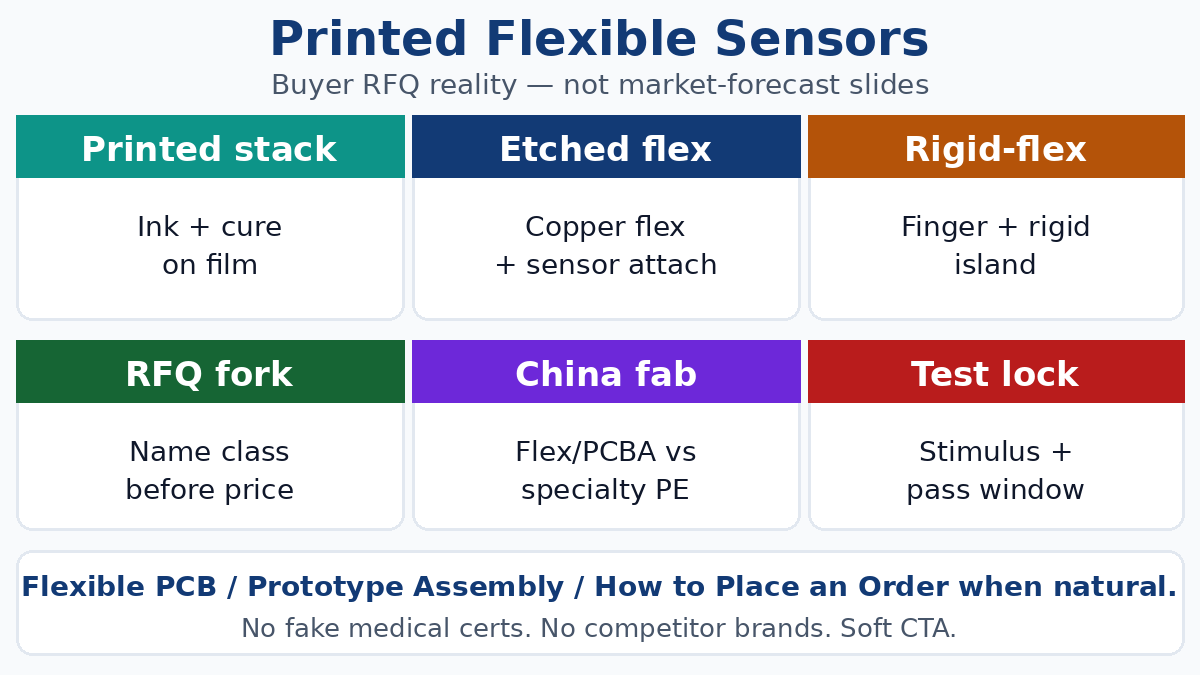
What “printed flexible sensor” should mean on an RFQ
For a purchasing or PE team placing work with an overseas China fab, “printed flexible sensor” is not a single traveler. It usually lands in one of three buckets — and awards fail when the RFQ mixes them without saying so:
- Printed sensor element on a flexible substrate — conductive / resistive / dielectric / functional inks deposited (screen, inkjet, gravure, or similar) to form electrodes, heaters, or sensing films. The “board” may never see subtractive etch the way a classic flex PCB does.
- Etched Flexible PCB as the interconnect — polyimide (or similar) flex with copper foil patterned by etch, then a discrete or module sensor attached by SMT / adhesive / connector. Sensing happens in the part; flex carries signals and power.
- Hybrid / rigid-flex system — sensor film or flex finger into a rigid section that holds MCU, power, and connectors. Rigid-Flex PCB rules apply on the interconnect side even when marketing still says “flexible sensor.”
Buyer failure mode: sending a “flexible sensor Gerber” that is really a printed ink stack, then expecting a conventional flex etch line to quote it as a commodity Flexible PCB lot. Write the construction class first — printed, etched flex + attach, or hybrid — before you argue price or turn time.
Printed vs etched flex vs rigid-flex — stop mixing travelers
Printed path. Electrodes and often the sensing film itself are deposited inks. Line resolution, sheet resistance, cure temperature, and adhesion to PET / PI / paper / stretchable films drive yield. Many of these builds never enter a copper-etch traveler. China PCB houses that run excellent polyimide etch may still be the wrong vendor if they have no printed-electronics process window.
Etched flex path. Copper on polyimide (single-sided, double-sided, multilayer flex) patterned by etch, coverlay / covercoat, stiffeners, and ZIF / FFC tails as needed. This is the lane most export flex fabs already know. A force / temperature / humidity / optical sensor then mounts as a component or subassembly. Depth on flex families belongs on the flexible-pcb-types lane; this page only needs the RFQ fork.
Rigid-flex path. When the product needs a bendy sensing finger and a rigid island for processing density, treat the interconnect as rigid-flex DFM — bend radii, coverlay openings, and bookbinder / air-gap notes — not as “just print it thinner.”
Practical split for buyers:
| Question | Printed sensor stack | Etched flex + sensor attach | Rigid-flex hybrid |
|---|---|---|---|
| Primary fab process | Ink deposit + cure | Copper etch + coverlay | Rigid + flex lamination |
| Typical file set | Print artwork, stack, cure notes | Gerber / ODB++ flex set | Rigid-flex stack + bend notes |
| Who often owns first article | Specialty PE / ink house or PE-capable fab | Export flex fab + PCBA | Rigid-flex capable fab + PCBA |
| Common RFQ mistake | Sending etch flex notes only | Ignoring ink cure / adhesion | Calling it “flex sensor” with no rigid notes |
Substrate, ink, and electrode stack — RFQ questions that matter
Do not invent XFPCB ink recipes or “we print any sensor” claims. Ask the questions that make two quotes comparable:
Substrate. PET, PI, PEN, paper, thermoplastic polyurethane, or other films — name the family, thickness, and whether the film must survive reflow, autoclave, sweat, solvent wipe, or outdoor UV. Stretchable vs bend-only matters for wearable straps.
Conductor / electrode. Silver, carbon, copper (printed or foil), PEDOT-family, or gold where required — sheet resistance target, line/space, and whether electrodes must remain solderable or only contacted by anisotropic adhesive / ZIF.
Functional / dielectric layers. Sensing chemistry (humidity, gas, biochemical, piezoresistive, capacitive touch) — who owns the formulation? Many medical / biosensor inks stay with specialty PE vendors even when the interconnect flex is China-fab friendly.
Stack order and cure. Print sequence, dry / cure temperatures, and whether later SMT heat will damage an earlier ink. Write max process temperature on the RFQ.
Barrier / overcoat. Moisture barrier, abrasion coat, or biocompatible skin-contact layers — specify pass/fail tests, not “medical grade” as a vibe.
Interconnect out. Does the sensor exit as a printed tail, etched flex tail, FFC, snap, or soldered pad field into a rigid board? That exit often decides whether Flexible PCB or a specialty PE house owns the first traveler.
When the stack is mostly copper-foil flex with ordinary SMT sensors, pull process windows from Technical Capabilities and keep ink questions short. When the sensing film is the product, treat ink / cure / adhesion as first-class RFQ lines — conductive-ink materials depth lives on the conductive-ink printed-electronics lane; keep this page on the buyer fork.
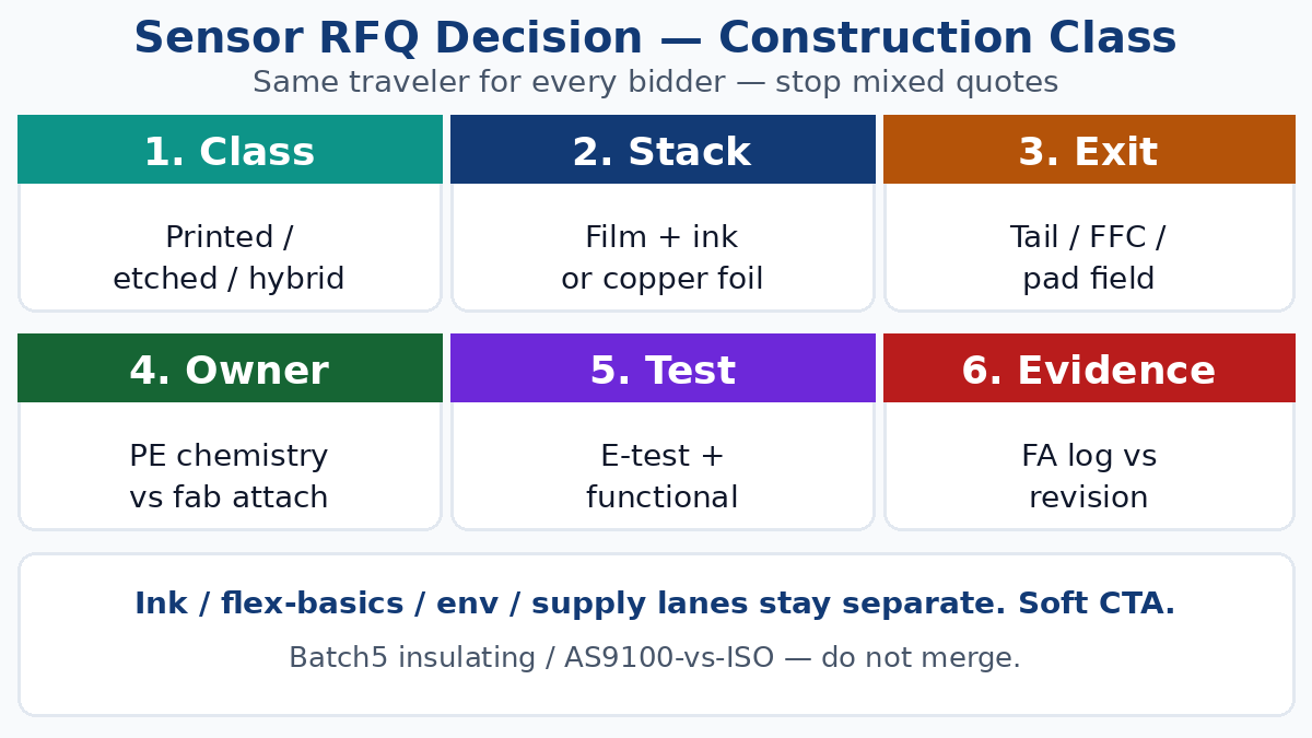
When China fab / PCBA can support vs specialty printed-electronics
Honest China fab voice: many export houses already run polyimide flex etch, stiffeners, coverlay, ENIG / OSP finishes, SMT, and AOI / flying-probe style electrical checks for interconnects that carry sensors. That is real capability for wearable hubs, HMI flex tails, and environmental-node boards where the sensor is a discrete or module.
What often stays specialty printed-electronics (or a dedicated PE line inside a larger group):
- Multi-layer functional ink stacks with proprietary sensing chemistry.
- Stretchable / textile-integrated electrodes outside the fab’s PI/PET window.
- Biosensor / electrochemical strips that need clean-room or reagent handling the PCB shop does not run.
- Ultra-fine printed features or roll-to-roll print that the local etch shop has never quoted.
Buyer practice: send a construction brief before the full Gerber dump. Ask the fab to confirm in writing: printed ink process available / not available; etched flex + SMT attach available; rigid-flex available. Silence is not a yes. For early builds that are etched-flex + attach, Prototype PCB Assembly and Quick Turn PCB are the natural service paths — not a promise that every printed biosensor belongs on the same line.
Kit risk is separate: if the BOM includes specialty sensor ICs, flex connectors, or adhesive films with long lead times, lock channel rules through Component Sourcing and keep calendar buffers on the supply-chain-issues lane — do not pretend this sensors page owns AVL depth.
Use cases without inventing XFPCB medical certificates
Printed and flexible sensors show up in medical patches, wearables, HMI / touch, and environmental / industrial sensing. Industry overviews are right that those markets are active. XFPCB honesty rules still apply:
- Medical / wearable skin contact. Ask for biocompatibility requirements your customer owns (ISO 10993 family tests, skin-contact declarations, sterilization method). Do not invent XFPCB ISO 13485, FDA, or CE medical device certificates on this page. If your product is a regulated device, your quality system owns that map — the fab RFQ owns construction, materials, and lot evidence against your revision.
- Wearable fitness / consumer. Bend life, sweat / laundry exposure, connector cycles, and battery flex routing matter more than a “medical” label. Specify dynamic bend counts and environmental exposure on the traveler.
- HMI / capacitive / force. Printed carbon / silver patterns on PET are common; resolution, optical clarity (if needed), and ESD / grounding notes belong on the RFQ.
- Environmental / industrial. Humidity, gas, temperature, and strain films — name the measurand, range, and calibration owner. Calibration is rarely “included free” with a bare printed film.
Do not invent AS9100 / aerospace sensor awards here either. If a program needs aerospace quality systems, that is a separate certification conversation — not a soft add-on to a printed-sensor brochure.
Specifying test and inspection
Soft language (“100% tested sensors”) is not award-ready. Write what fails the lot:
- Dimensional / registration — electrode pattern vs substrate datum; print-to-print overlay if multi-pass.
- Electrical — sheet resistance / continuity / isolation on electrode nets; flying-probe or dedicated fixture where the construction allows. Route method language through PCB board testing and inspection when the interconnect is a conventional flex / rigid-flex board.
- Functional / golden-sample — for sensing films, define stimulus (known humidity, force, gas concentration, or electrical proxy) and pass window. State who owns the fixture: buyer, fab, or third party.
- Adhesion / bend — tape test, mandrel bend, or cycle count for dynamic wearables — numbers on the RFQ, not “flexible enough.”
- Cosmetic — pinholes in overcoat, ink voids, scratches that affect contact pads.
For SMT-attached sensors on etched flex, AOI / X-ray rules follow the assembly class you already use elsewhere; do not invent a special XFPCB “sensor AOI certificate.” Freeze the file set via Manufacturing Files before first-article arguments about print artwork versus Gerber layers.
RFQ paste — what to lock before award
Copy and adapt (write your own numbers; do not invent XFPCB TAT or capability IDs):
- Construction class — printed ink stack / etched flex + sensor attach / rigid-flex hybrid — pick one primary path.
- Substrate family + thickness — PET / PI / other; max process temperature; stretch vs bend-only.
- Electrode / ink notes — conductor type, sheet-resistance target, line/space, cure limits; or “copper foil etch per flex stack note.”
- Sensor ownership — sensing chemistry / module P/N owned by buyer vs fab-sourced; AVL / channel rules if turnkey.
- Exit interconnect — printed tail / etched flex / FFC / soldered pad field into rigid.
- Test matrix — dimensional, electrical, functional stimulus + window, bend / adhesion as applicable.
- Evidence — first-article photos, resistance map, functional log against revision — not a homepage “sensor capable” badge.
- Environment / substance — RoHS / REACH gates when your market requires them (environment lane owns depth; keep a one-line pointer here).
Route award logistics through How to Place an Order only after construction class and test matrix are frozen — not after a soft “flexible sensor” line reopens the traveler post-PO.
China fab honesty — what this page will not claim
Capable export flex and PCBA houses routinely support etched Flexible PCB interconnects, stiffeners, connector tails, SMT sensor attach, and hybrid rigid-flex for wearable hubs, HMI, and industrial nodes. Some groups also run or partner for printed conductive patterns on PET/PI. That still is not a license to invent:
- XFPCB market-size leadership or “$X billion sensor plant” claims.
- Fake ISO 13485 / FDA / CE medical device certificates.
- Fake AS9100 / aerospace printed-sensor awards.
- Universal “we print any biosensor chemistry” capability.
Prefer written construction class + process window + test matrix over pride logos. When the sensing chemistry is proprietary specialty PE, say so early and split the PO: printed element from the PE vendor, interconnect / PCBA from the China fab that actually owns that traveler.
Soft next step
If your next lot is etched flex or rigid-flex interconnect with sensor attach, start from Flexible PCB or Rigid-Flex PCB, freeze files under Manufacturing Files, and use Prototype PCB Assembly for first articles. If the stack is truly printed functional ink, ask the fab to confirm the print process in writing before you treat it as a commodity flex RFQ. Place the award path through How to Place an Order when construction, kit, and test gates are locked — not when a market-forecast slide is the only document on the table.