
Search results for “PCB lithography” often land on semiconductor wafer stories: UV exposure through a photomask onto silicon, then a market note about equipment growth. That framing mixes two different factories. PCB photoimaging (also called PCB photolithography in fab talk) patterns copper on laminated cores and outer foils. Wafer lithography patterns nanoscale features on silicon dies. Buyers who treat those as the same process write RFQs that omit the fields China CAM actually uses to protect yield — minimum trace/space, annular ring, registration windows, and whether the critical geometry sits on inner layers or outer. This factory buyer guide separates the two, walks resist → expose → develop → etch as it runs on a PCB line, compares LDI versus film artwork, and lists RFQ notes that keep imaging scrap out of your SMT lot. It is not a wafer process textbook and it does not invent market-size forecasts.
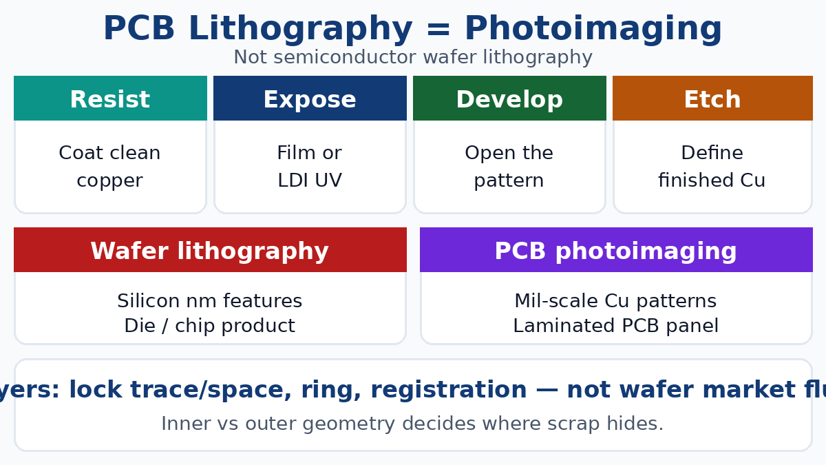
PCB photoimaging is not wafer lithography
Both processes use light-sensitive resist and patterned exposure. That is where the useful overlap ends.
Wafer lithography projects circuit images onto silicon wafers at feature sizes measured in nanometers. It relies on complex optics, photomasks (or maskless steppers in some flows), cleanroom classes that dwarf a typical PCB imaging room, and process control aimed at transistor and interconnect yield on a die. The “board” is the wafer; the end product is a chip, not a laminated interconnect panel.
PCB photoimaging coats copper-clad laminate with photoresist, exposes a circuit pattern at mil-scale geometries, develops away unwanted resist, and etches (or plates-and-etches) copper where the resist no longer protects. Inner layers are imaged before press. Outer layers are imaged after drill and plate on a multilayer blank. The acceptance language is IPC fab criteria, annular ring, and etch undercut — not EUV tool roadmaps.
Conflating the two creates three buyer mistakes. First, quoting “lithography capability” as if a PCB shop’s LDI line were a semiconductor toolset. Second, skipping PCB-specific RFQ fields because a wafer article never mentioned annular ring or inner-layer registration. Third, expecting equipment-growth market fluff to tell you whether your 4/4 mil stack will etch cleanly on a China traveler. It will not.
For procurement and hardware leads, the practical definition is simple: PCB lithography here means the photoimaging steps that turn Gerber copper into surviving copper on the panel. Everything else in this article supports that definition.
Resist → expose → develop → etch (buyer view)
You do not need bath chemistry charts to buy boards well. You need to know which step fails when a note is missing.
1. Clean and coat. Copper surface is cleaned; liquid or dry-film photoresist is applied. Dry film is common on many rigid lines; liquid resist appears where process recipes demand it. Contaminated copper or uneven coat shows up later as pinholes, resist lift, or etch nicks — defects that look like “etch problems” on AOI but started at coat.
2. Expose. The circuit image is transferred into the resist with UV. Artwork arrives as plotted film (diazo/silver film on glass or polyester) or as a digital file driven on a laser direct imaging (LDI) head. Exposure dose and focus/registration decide whether fine traces hold and whether pads sit where the drill expects them. Outer and inner exposure may use different tools and different compensation tables.
3. Develop. Unwanted resist washes away, leaving a copper mask of the circuit (or a plating mask, depending on pattern-plate vs panel-plate flow). Under-develop leaves scum that blocks etch; over-develop undercuts fine features. Develop windows are process capability, not a free checkbox on a capability PDF.
4. Etch (and related outer flows). Exposed copper is removed where resist no longer protects, or plating builds where resist allowed, then flash etch finishes the geometry. Etch factor and undercut set how much a drawn 4 mil line shrinks relative to the artwork. CAM applies etch compensation from historical line data — another reason “min trace on the drawing” and “min trace that survives etch” are related but not identical.
5. Strip and inspect. Resist is stripped; inner layers go to AOI before they disappear forever inside the press. Outer layers continue to mask and finish after pattern definition. An open that escapes inner AOI becomes buried scrap; an outer nick that passes soft visual can still fail electrical test or fail after thermal stress.
From a buyer seat, this sequence matters because every RFQ claim about “fine line” is really a claim about coat uniformity, exposure registration, develop latitude, and etch control working together. Naming only “LDI available” without min trace/space, copper weight, and registration notes leaves the estimator to guess which process window you meant.
LDI vs film — what changes for the RFQ
Film imaging plots Gerber to physical artwork, then contacts or projects that film onto the panel. It is still used widely, especially where geometries sit comfortably inside film capability and volume amortizes plot cost. Film introduces art-plot tolerances, film stretch/shrink with humidity and handling, and contact defects (dust, scratches) that print as opens or shorts.
Laser direct imaging (LDI) writes the pattern from CAM data onto the resist without a plotted film intermediary. Typical buyer-visible benefits: tighter registration to panel fiducials, easier scale and compensation per panel, and fewer film-handling defects on fine features. LDI is not automatic magic. It still needs correct CAM compensation, clean coat, correct dose, and etch that matches the compensated artwork. A shop that owns LDI but quotes your job on a film line without saying so has changed the process you thought you bought.
| Topic | Film artwork | LDI |
|---|---|---|
| Artwork | Plotted film per layer | Digital from CAM |
| Registration | Film + aligner stackup | Panel fiducial / camera driven |
| Fine-line comfort | Process- and plot-limited | Often preferred for tight geometries |
| Volume economics | Plot NRE / film wear | Machine time; less film stock |
| Buyer RFQ ask | Confirm film vs LDI for critical layers | Confirm which layers run LDI |
Write the imaging method when fine pitch, HDI outer, or tight soldermask registration rides on the same panel. If the quote is silent, ask. Silent defaults are how two China quotes diverge on the same ZIP.
Inner versus outer also matters. Inner layers are imaged on cores before lamination; registration error becomes layer-to-layer shift sealed in the stack. Outer imaging must register to drilled holes so annular ring survives. A board can meet outer min-trace marketing while failing annular ring because drill and outer image never shared a locked compensation story.
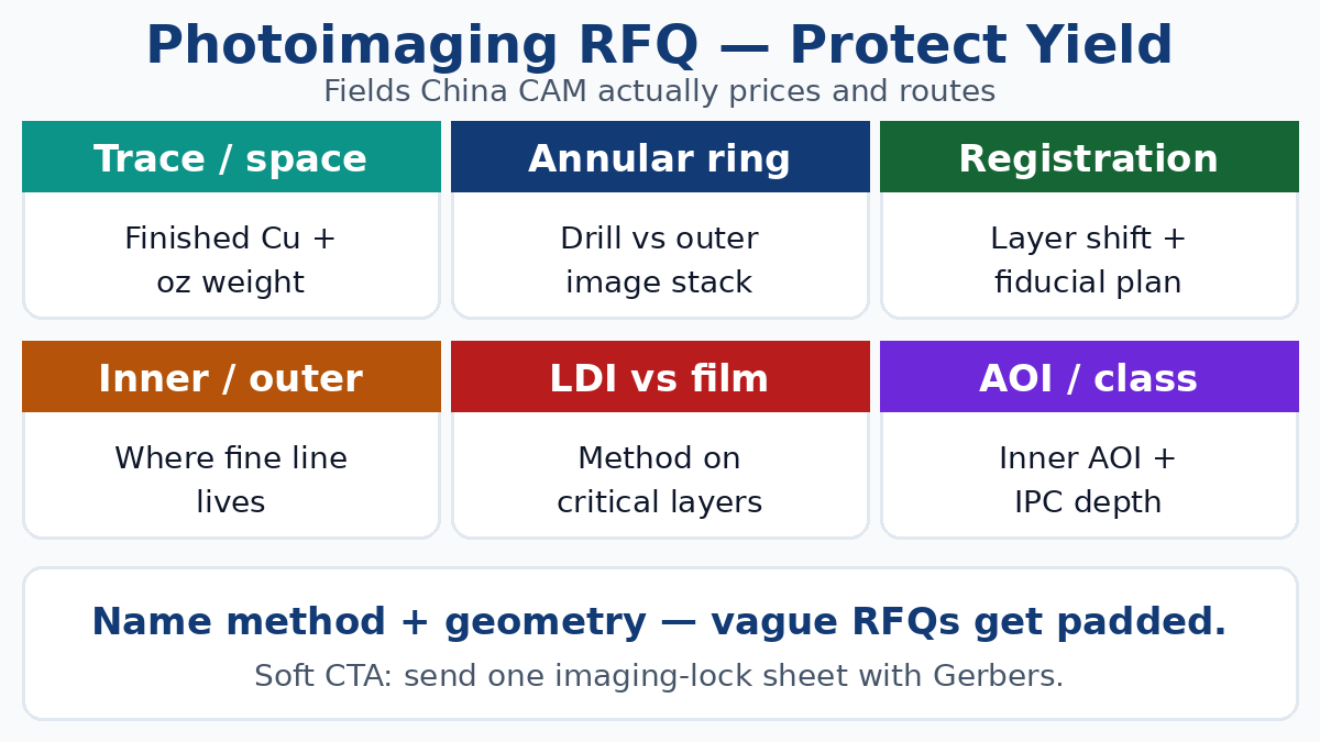
RFQ fields that protect imaging yield
Put these on the fab drawing or RFQ package. Do not leave them as brochure adjectives.
Minimum trace and space. State finished copper geometry after etch, copper weight per layer, and whether the critical nets are inner or outer. “3/3 mil capable” on a website is not the same as “this job is designed and accepted at 3.5/3.5 on 1 oz outer.” Ask for the process window the shop will run for your copper weight — not the marketing floor.
Annular ring. Minimum annular ring on plated holes ties drill accuracy to outer (and sometimes inner) image registration. Tight rings with large drill tolerance stacks fail as breakout even when traces look fine on AOI. Call Class-driven ring expectations explicitly when reliability needs them.
Registration / layer-to-layer. Multilayer jobs need a registration budget: how cores and outer images align after press and drill. Sequential lamination and HDI multiply registration risk. If you have impedance coupons or critical pad-to-via relationships, say so; CAM compensation and coupon placement follow from that.
Inner vs outer critical features. Call which layers carry the tightest geometries. Inner fine line that escapes AOI is expensive scrap. Outer fine line that fights mask dams becomes SMT bridges. Treating all layers as one “min feature” number hides where the shop must spend process control.
Copper weight and etch compensation ownership. Heavier copper widens undercut and changes how aggressive compensation must be. Confirm whether CAM applies shop compensation tables and whether you must draw to finished or to artwork dimensions. Mixed language here produces mixed quotes and EQ loops.
Imaging method for critical layers. Film or LDI; contact notes for soldermask if mask registration is equally critical. Mask imaging is a sibling process — still photoimageable on most LPI lines — and mask dams often decide whether fine outer copper is assemblable.
AOI and electrical test depth. Inner AOI before press, outer AOI, and netlist electrical test catch different failure modes. Imaging scrap that only shows after press is a calendar and money failure. Write whether 100% inner AOI is included for your layer count.
Acceptance class. IPC visual and performance depth change how much annular breakout, nick, or etch irregularity is acceptable. Class language without imaging notes is incomplete; imaging notes without class language leave FQC arguing from habit.
When two quotes diverge on the same Gerbers, ask each vendor which of the fields above were assumed as house defaults. The honest list beats a softer unit price.
China fab practical notes (photoimaging traveler)
Overseas buyers sourcing from China fabs feel imaging risk most when files are fine-line, multilayer, or mixed copper — and when English RFQs use wafer vocabulary.
EQ language. CAM will ask about min trace/space versus copper ounce, unclear plated-hole attributes, conflicting stack notes, and whether impedance lines were drawn pre- or post-compensation. Answer with revision-controlled notes. Chat screenshots are not a traveler update. An unanswered EQ parks the panel; a vague “use your standard lithography” answer invites the cheapest compliant-looking window, not the one your layout assumed.
Capability vs traveler. Many shops publish aggressive fine-line capability. The traveler for your PO may still route to a film line, a wider etch recipe, or a looser AOI sample if the RFQ never locked method and acceptance. Ask which process family your price assumes. If LDI is required for outer fine pitch, write it.
Inner AOI discipline. China multilayer lines that skip or sample inner AOI to hit a low quote push risk into buried layers. For dense inners, treat inner AOI inclusion as a quote field, not a courtesy. Escapes found only at flying probe — or worse, at SMT — cost more than the AOI minutes saved.
Humidity, film, and schedule. Film-based jobs are more sensitive to artwork age and storage. LDI reduces that vector but still needs stable coat and develop. Expedite premiums buy queue position; they do not rewrite etch physics. Changing copper weight or min-space after CAM freeze resets both imaging compensation and often the price.
Mask and finish coupling. Photoimaging does not end at copper. Soldermask LPI imaging registration decides dam width on fine pitch. Finish choice does not fix a misregistered image. Keep copper imaging notes and mask registration notes on the same RFQ so fab and assembly arguments do not bounce between vendors.
Revision lock. China fabs build the revision on the PO. If layout tightens traces after quote but the PO still says Rev A, Rev A imaging compensation may still run. Update files and PO together when geometry that affects etch or registration changes.
None of this requires inventing plant counts or dollar menus. It requires naming the imaging contract the same way you already name finish and class.
What this guide deliberately skips
This is not an end-to-end fab traveler. Drill aspect ratio, surface-finish menus, packing docs, and assembly scrap economics belong in broader fabrication and sourcing write-ups. Here the scope stays narrow on purpose: stop wafer/PCB conflation, make photoimaging steps readable for buyers, separate LDI from film, and lock the RFQ fields that decide whether copper patterns survive etch and registration. If your debate is really about finish shelf life or Incoterms, those notes still matter — they just do not replace imaging geometry on the drawing.
Soft next step
Before the next fine-line or multilayer RFQ, add a one-page imaging lock to the fab package: finished min trace/space by copper weight and by inner versus outer, minimum annular ring, registration or layer-shift expectations, film versus LDI for critical layers, etch-compensation ownership, inner AOI inclusion, and IPC class. Send that sheet with Gerbers or ODB++ to every bidder.
When those fields are explicit, a China fab can price and route a real imaging process instead of padding unknown lithography risk. Share the open questions early, freeze geometry before CAM compensation locks, and treat photoimaging notes as yield insurance — not as optional lab jargon borrowed from a wafer article.