
Leadless IC packages show up on RFQs as “QFN OK,” “DFN same as QFN,” or “LGA like BGA without balls.” Those shortcuts skip the real buyer work: which leadless family you actually bought, how the footprint and exposed pad land on the PCB, how paste and stencil set joint volume, and which inspection methods can see under the body after reflow. This page is a factory/buyer leadless package guide for PCB and PCBA — QFN, DFN, LCC, and LGA as a family overview, plus footprint, thermal-via, stencil, tombstone/void, and China fab-plus-assembly RFQ locks. Soft CTA only. A separate XFPCB lane already owns soldered land-grid-array pad/paste/X-ray depth — name LGA here as one leadless type in prose; do not clone that deep dive. No competitor brands. No invented XFPCB capability menus.
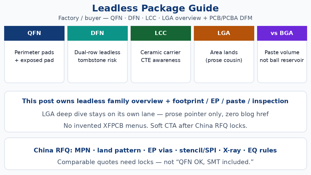
What “leadless” means on a PCB RFQ
A leadless package is a surface-mount IC that does not use classic external leads (gull-wing, J-lead, or through-hole pins). Electrical connection is through flat conductive pads on the package bottom and/or metallized edges. The joint forms between those pads and the PCB land pattern during SMT reflow (or, for some ceramic carriers, with process notes the datasheet already owns).
Buyers care because short electrical paths cut package inductance and resistance versus long leads — useful for dense boards, power devices with bottom heat paths, and many mid-frequency digital/RF parts. The same geometry hides most joints under the body after reflow, so paste volume, coplanarity, and inspection method become first-class PO language instead of “SMT included.”
Leadless is a family, not one footprint library entry. Treating every bottom-terminated part as interchangeable paste and pad practice is how first articles open, bridge, or void under the thermal pad.
Leadless family map: QFN, DFN, LCC, LGA
Use datasheet package names, not marketing nicknames:
| Type | Typical termination | What buyers usually lock |
|---|---|---|
| QFN (quad flat no-lead) | Perimeter pads on four sides + often a large center exposed pad (EP / thermal pad) | Land pattern, EP paste fraction, thermal vias, stencil thickness |
| DFN (dual flat no-lead) | Perimeter pads on two sides + often a center EP | Same pad/paste discipline as QFN; easier tombstone risk on small dual-row bodies |
| LCC / LCCC (leadless chip carrier / ceramic) | Bottom terminals, often with side metallized castellation on ceramic | CTE vs PCB, hermetic / high-reliability notes, pad geometry from drawing |
| LGA (land grid array) | Area array of flat lands under the body (socketed or soldered) | Pad/paste/flatness/hidden-joint inspection — soldered LGA depth lives on the dedicated LGA guide; here it is one leadless cousin |
PQFN / similar plastic QFN-style names in catalogs usually still mean perimeter pads plus a bottom exposed pad. Confirm the MPN drawing; do not assume “P” changes your pad set.
Vs packages with balls. Pre-attached solder balls (as on a BGA PCB program) bring a solder reservoir on the component. Leadless packages generally do not — PCB-side paste largely sets joint volume and stand-off. Ball escape, mask, and collapse language does not automatically translate to QFN/DFN aperture recipes.
Vs leaded SMT (QFP, SOP). Gull-wing leads give optical access to heel/toe fillets and more forgiveness on Z coplanarity. Leadless trades that visibility for density and thermal path — and for under-body inspection discipline.
Mention LGA in RFQs when the BOM actually is an LGA. Do not paste BGA ball-process notes onto QFN, or QFN EP paste rules onto a fine-pitch LGA array, without reading the drawing.
Footprint and pad design that survives DFM
Reliable leadless assembly starts with the component manufacturer’s recommended land pattern, not a generic “QFN 5×5” CAD library part that someone resized once in 2019.
Lock on fab / assembly notes:
- Pitch, pad length/width, and toe/heel extensions exactly as the package drawing (or IPC-derived pattern the PE already approved for that MPN)
- Solder-mask-defined vs non-solder-mask-defined as datasheet calls — local “improve the mask” habits break fine-pitch QFN
- Mask opening and registration vs pitch; fine pitch leaves little room for mask shift
- Surface finish compatible with wetting on small pads (finish type and any thickness expectation your process card already uses)
- Via rules under pads — especially under the exposed pad: via-in-pad fill/cap policy, or dog-bone, written so CAM does not invent a cheap open via that steals solder into the barrel
Two QFNs with the same outline can still need different pad sets. Outline similarity is not a process win.
Dense perimeter pitch or area-array cousins often push escape into microvia territory. When fanout is truly high-density interconnect work, say so in prose with HDI process language (laser vias, sequential build-up, via-in-pad policy) instead of hoping a standard through-hole multilayer quote absorbs the escape. Do not invent XFPCB layer or microvia menus here — write the via and density gates; let DFM answer against the files.
Exposed pad, thermal vias, and heat path
Many QFN/DFN (and related) packages put a large exposed pad on the package bottom. That pad is usually ground and/or the primary thermal path from the die to the PCB copper.
Buyer locks that matter:
- PCB thermal land size matching the datasheet recommendation (including any solder-mask web or segmented pad notes)
- Thermal via pattern — count, diameter, plating, and whether vias are filled/capped when paste sits over them
- Paste coverage fraction on the EP (often a windowed or reduced aperture, not 100% flood — follow the package or assembler-approved plan)
- Void expectations if thermal or reliability criteria care about EP void area
Uncontrolled vias under a big EP wick paste into barrels, raise void area, and can starve the joint. Put EP paste and via notes on the assembly drawing, not only in a buried CAD property.
Thermal performance is a system: package EP + PCB copper pour + vias + airflow / chassis. A pretty via pattern does not replace a written copper and paste plan.
Stencil, paste, and SPI — volume without balls
Because most leadless parts do not bring BGA-style balls, PCB-side solder paste largely sets joint volume.
Failure modes buyers should recognize:
- Too little paste on perimeter pads → opens, weak joints, extreme sensitivity to package tilt
- Too much paste → bridging between fine-pitch pads, solder smear
- Wrong EP aperture → large voids, die attach thermal risk, or EP solder shorting to nearby pads
- Uneven print height across a small DFN/QFN → one side wets; the other tombstones or opens
Stencil thickness, aperture size/shape (home-plate, windowpane on EP, etc.), and paste type must follow the footprint — there is no universal “QFN stencil.” For fine-pitch or reliability builds, require 3D SPI before placement so volume and offset get caught before reflow hides the evidence.
Ask the assembler to state stencil thickness class, EP vs perimeter aperture strategy, paste alloy/type, and whether SPI is in-process or sample-only. “SMT included” without paste language is not a leadless process lock.
Tombstone, void, and other defect language
| Symptom | Typical contributors | Why buyers care |
|---|---|---|
| Tombstone / drawbridging (esp. small DFN) | Uneven paste, pad imbalance, placement offset, uneven heating | Open on one terminal; optical catch possible if body tilts |
| Perimeter open | Low paste, non-wetting, coplanarity, warp | Hard to see under body; field intermittent |
| Bridge | Excess paste, print offset, misplace | Short under or at pad edges |
| EP voiding | Outgas, via wicking, flood paste, profile | Thermal and reliability risk if large / clustered |
| Misalignment | Placement, datum, wrong footprint | Partial pads, bridges |
Small dual-row DFN and tiny chip-scale leadless parts are classic tombstone candidates when pad copper or paste volume is asymmetric. Fix pad/paste balance and thermal balance — do not only “slow the conveyor” without a written root cause.
Translate defects into PO language: SPI gates, X-ray sample plan for hidden joints / EP voids, and acceptance criteria — not “good workmanship” alone.
Assembly flow and inspection buyers should recognize
A normal leadless path inside PCB Assembly looks like:
Paste print → SPI (when required) → place → reflow → inspect → electrical / functional test
Placement accuracy tightens as pitch shrinks; self-centering from long leads is limited. Reflow follows paste and component limits plus board thermal mass — not a marketing “QFN profile.” Lead-free vs tin-lead, nitrogen vs air, and soak/peak windows belong on the process card for the MPN.
After reflow, perimeter fillets may be partly visible; most EP and inner-array joints are under the package.
- AOI checks presence, polarity/marking where visible, gross placement, and exposed defects. It does not fully characterize the hidden EP joint.
- X-ray is the usual tool for hidden joint shape, bridges under the body, and EP void signatures. Use the live X-ray inspection lane when you need that method named on the PO — do not assume every quote includes it.
- Electrical test finds opens and shorts the netlist can see. It does not prove void percentage.
When X-ray still helps even if the board boots: first articles on fine-pitch QFN/DFN, EP void concerns, process changes (new stencil, paste lot, fab lot), and reliability expectations that care about joint structure. Imaging confirms symptoms; it does not rewrite a wrong land pattern.
Ceramic LCC / LCCC programs add CTE mismatch awareness between ceramic and organic PCB — temperature cycling and solder joint fatigue belong on the reliability plan when the application is high-reliability, not only on a brochure “hermetic” adjective.
China fab + assembly RFQ locks
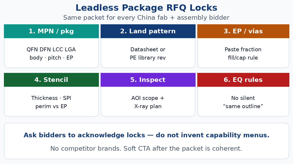
Export quotes diverge when language stays soft (“QFN OK,” “leadless SMT,” “thermal pad standard”). Paste comparable locks so every bidder answers the same traveler. Attach Gerbers/ODB++, BOM, centroid, and assembly drawings with Manufacturing Files before “SMT TBD” quotes are treated as comparable.
- MPN and package drawing — exact package name (QFN/DFN/LCC/LGA), body size, pitch, and EP dimensions. No “or similar outline.”
- Land pattern ownership — datasheet pattern or PE-controlled library revision on the fab notes.
- EP / thermal pad plan — paste coverage intent, via pattern, fill/cap rule if paste overlays vias.
- Stencil / paste class — thickness class, perimeter vs EP aperture strategy, paste alloy/type, SPI yes/no.
- Surface finish — called separately; leadless wetting is not “whatever ENIG the fab has.”
- Inspection method — AOI scope; X-ray sample or 100% for hidden joints / EP voids; electrical / functional ownership.
- Warpage / thickness notes when thin boards or large packages share the panel.
- Lock vs PE-approved equivalent — package or footprint substitutes need signed EQ; silent “same size QFN” swaps refused.
- No invented menus — do not paste competitor brand ads or invent XFPCB stencil, void %, or TAT claims. Generic process locks are enough for comparable RFQs.
Quick-turn PCB fabrication and assembly can still run leadless parts when the locks above are coherent — speed does not replace EP paste notes. Name quick-turn only when the schedule is real; do not treat rush as a substitute for DFM.
Buyer mistakes that burn leadless awards
“QFN OK” with no MPN land pattern. Outline is not a footprint.
Copying a BGA stencil reduction onto QFN/DFN. Ball volume and land volume are different problems.
Flooding the EP at 100% paste with open vias underneath. Classic void and wicking farm.
Assuming AOI alone closes fine-pitch leadless. Hidden EP joints need a written inspection method when reliability cares.
Cloning soldered LGA pad/paste depth into every QFN RFQ — or the reverse. LGA is one leadless type with its own array geometry; QFN/DFN EP rules are not a drop-in substitute for area-array land process notes.
Awarding on unit price before paste, via, and X-ray gates match. The cheap line that skipped SPI and EP via fill often returns as scrap under the body.
Soft close
When the BOM is leadless, freeze package identity, land pattern, exposed-pad paste and vias, stencil/SPI expectations, and inspection method before price comparison. XFPCB can review coherent fab-plus-assembly packets against those locks — start from How to Place an Order when the traveler is ready. Soft CTA only; no invented capability scorecards. Send the drawings and the traveler language together so DFM answers the board you actually built, not the nickname on the RFQ subject line.