
Low Dk and low Df show up on every RF and high-speed RFQ, then get treated like a brand slogan. Buyers ask for “low-loss laminate,” fabs reply with a datasheet headline measured at a convenient frequency, and nobody locks whether that number is the modeling Dk for impedance, the Df that owns insertion loss at the channel band, or a marketing pair that will never match the pressed stack. This page owns the factory/buyer selection frame for low Dk / low Df PCB materials: what Dk and Df actually mean for delay and loss at buyer level, when to leave FR-4-family glass-epoxy, hybrid stack notes that China fabs can build, copper foil and roughness honesty, and RFQ locks that name targets, construction, and impedance. Soft CTA only. Sibling XFPCB lanes already cover lead-free Tg vs when FR-4 is enough, core/prepreg/bondply roles, cross-family selection gates, and insulating-materials callouts — name those lanes in prose; do not clone or href them. Process depth for microwave builds sits on the High Frequency product page. No competitor brands. No invented XFPCB warehouse grade menus or lab Dk tables.
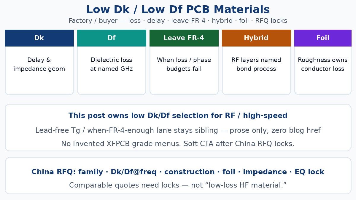
What Dk and Df mean at buyer level
Dielectric constant (Dk, εr). Dk sets how fast a signal travels in the dielectric and how wide a trace must be for a target impedance at a given dielectric height. Lower Dk → faster propagation (lower delay per length) and usually wider geometry for the same impedance on the same thickness. Buyers care because impedance coupons, skew budgets, and filter timing all assume a modeled Dk — not a brochure nickname. If two bidders quote “Dk ~3.5” without frequency, glass style, resin content, or the stack calculator assumptions, those quotes are not comparable.
Dissipation factor (Df, loss tangent). Df measures how much energy the dielectric turns into heat as the field switches. At rising GHz, dielectric loss often dominates channel budgets before copper DC resistance does. Lower Df → less insertion loss per length at a named frequency. Buyer failure mode: awarding on a friendly Df at 1 GHz when the eye or PA path lives at 6–28 GHz. Df without a frequency is decoration.
How they interact on the traveler. Dk mainly owns geometry and delay; Df mainly owns dielectric loss. Both move with frequency, temperature, resin content, and glass weave. Neither freezes Tg, CAF immunity, peel strength, or lead-free reflow survival. Lead-free thermal reality and “when FR-4 is enough” already sit on the sibling lead-free / HF lane — this post assumes you already know Tg/Td are a separate lock, then asks whether the electrical family must leave FR-4 at all.
For controlled-impedance programs, pair dielectric honesty with Impedance Control PCB process ownership: modeled Dk at the fab’s calculator frequency, pressed thickness, and coupon ownership when the program needs measured evidence — not only CAM estimates.
When FR-4-family is still enough
Not every multi-gigabit or RF-adjacent board needs specialty low-loss laminate. Stay on FR-4-family (including lead-free, high-Tg grades) when:
- Channel length and edge rates keep insertion-loss budgets inside what FR-4-family Df can hold at your named frequencies after honest stack modeling
- Impedance targets are achievable with documented core/prepreg thickness, glass style, and a modeled Dk the fab will press to
- The design is mixed-signal / digital with real GHz content that is not microwave front-end or mmWave critical
- Hybrid RF layers are not already in the electrical plan
In that band, buyer work is honesty work: freeze modeling frequency, freeze stack notes, refuse silent “FR4 or equivalent” resin swaps. Ordinary multilayer rigid builds under PCB Manufacturing menus often default to FR-4-family in China export quotes — fine when the loss gate fits, a failure mode when the RFQ never tested loss at the band you ship.
When to leave FR-4 for low Dk / low Df families
Open a true low-loss conversation — enhanced epoxy / mid-loss, PPO-PPE / hydrocarbon blends, PTFE / ceramic-filled ultra-low-loss, or hybrid — when any of these are real on the program, not when a marketing page prefers an adjective:
- Insertion loss, eye, or phase budgets fail on FR-4-family at named frequencies after stack modeling that uses honest Df
- Dk stability vs frequency and temperature is part of the channel budget (filters, matched RF paths, tight skew / length matching)
- Hybrid stack (FR-4-family digital layers + low-loss RF layers) is already the electrical plan
- Copper roughness, glass weave, and resin-content effects dominate at your band and commodity FR-4 process windows cannot hold the tolerance
That gate belongs on High Frequency PCB process ownership: material family, drill/plate/bond deltas, impedance and inspection notes — not a blog slogan that “HF FR-4 equals specialty low-loss.” Do not invent XFPCB stocked grade menus. Write family and property gates; let DFM confirm process fit against the files you send.
Rough buyer bands (illustrative, not a stock list). Mid-loss enhanced epoxy systems often land roughly Dk ~3.2–3.6 with Df ~0.006–0.010 @ 10 GHz-class test points — useful when FR-4 Df is the limiter but PTFE process cost is not justified. Hydrocarbon / PPO-PPE blends often land roughly Dk ~3.0–3.3 with Df ~0.003–0.006 — common for multi-gigabit SerDes and Sub-6 RF where loss budgets tightened. PTFE / ceramic-filled ultra-low-loss systems often land Dk ~2.1–2.6 with Df ~0.001–0.002-class — needed when mmWave, long RF paths, or phase budgets refuse FR-4-family loss. These ranges are selection grammar, not XFPCB warehouse SKUs. Named brands belong only when your controlled document already specifies them.
Hybrid stack notes buyers actually need
Hybrid boards place low-loss (often PTFE or ceramic-filled) layers where RF paths live and FR-4-family layers where digital / power density and cost matter. That is a process change, not a checkbox.
Buyer notes that prevent award shock:
- Name which layers are specialty. “Hybrid low-loss” without layer callouts invites the fab to guess — or to quote FR-4 everywhere and surprise you at CAM.
- Bondply / prepreg chemistry. PTFE-to-FR-4 bonds need compatible bond films or process-qualified prepregs. Core vs prepreg vs bondply roles already live on the laminates-and-adhesive-sheets sibling lane — freeze construction intent here; do not re-teach stack grammar.
- Drill, desmear, and plate deltas. PTFE and some ceramic-filled systems need different plasma / desmear and plating windows than FR-4. Ask whether the quoted house has run the family before on similar stack thickness — without inventing a capability menu.
- CTE and press cycles. Mixed families can shift registration and bow/twist risk. Lock overall thickness, copper weights, and press notes with the stack traveler.
- Impedance reference layers. State which layers carry controlled impedance and which dielectric Dk the calculator must use per region. One global “Dk 3.5” across a hybrid stack is a common CAM failure mode.
Hybrid is priced and scheduled as a process family change. Write it explicitly on the RFQ; do not bury it in a drawing note the buyer never paste into the quote packet.
Copper foil and roughness — honesty without hype
Dielectric Df is only half of high-frequency loss. Copper foil roughness (tooth / treatment profile) adds conductor loss that rises with frequency as skin effect pushes current into the copper-dielectric interface. Buyers who lock “low Df laminate” and leave foil type as “standard ED” often discover the channel still fails at mmWave or long SerDes runs.
Honest buyer practice:
- Ask whether the stack assumes standard electrodeposited (ED) foil, reverse-treat / low-profile, or ultra-low-profile foil on RF / high-speed layers
- Do not assume “low Dk laminate” automatically ships with low-profile copper — foil is often a separate traveler line
- Roughness impact grows with frequency and with how much of the current sits against the treated side; short digital stubs care less than long RF microstrips
- Foil choice can change peel, etch factor, and impedance geometry slightly — lock it with the stack note when loss budgets are tight
This is not a free upgrade demand. Refuse to pretend dielectric Df alone owns GHz insertion loss. Mention foil class when the channel needs it; skip it when FR-4 indicators are the whole job.
Frequency, resin content, and datasheet traps
Dk and Df move with frequency. A laminate rated Dk = 3.50 at 1 GHz may read lower at 10 GHz while Df rises. Always request frequency-specific data near your band — or accept that the fab’s stack calculator uses a modeled value that must be written on the traveler.
Resin content and glass style change effective Dk. Higher resin / lower glass often lowers effective Dk and can shift Df; weave style drives anisotropy and fiber-weave skew on differential pairs. Two cores with the same family nickname and different resin content are not the same dielectric for impedance. Pressed reality beats datasheet headline.
Test method matters. Fixture differences can move reported Dk/Df. You do not need to litigate metrology on every RFQ — bidders must acknowledge the same modeling frequency and stack assumptions so quotes share one traveler.
Lead-free thermal class is still a separate lock. Low Df does not buy Tg/Td. A PTFE or hydrocarbon system can still need explicit reflow exposure notes. Keep thermal locks on the lead-free / FR-4 sibling frame; keep electrical family locks here.
China fab RFQ locks for low Dk / low Df awards
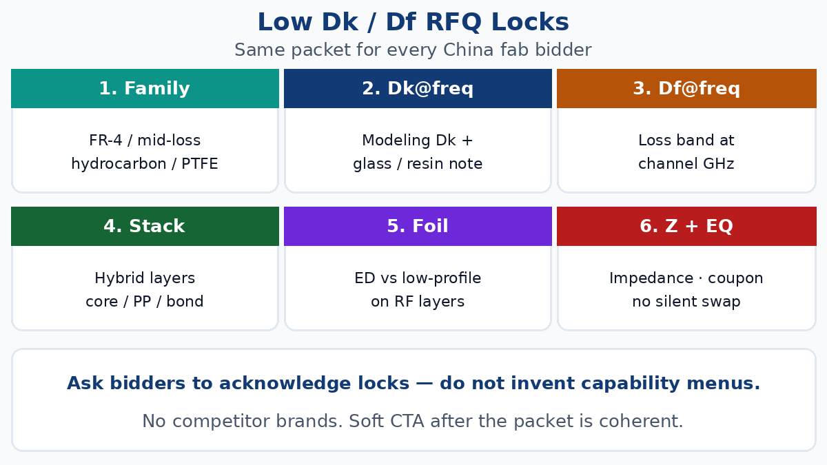
Export quotes diverge when material language stays soft (“low-loss FR4,” “HF material,” “or equivalent”). Paste comparable locks so every bidder answers the same traveler. Attach stack notes and Gerbers/ODB++ with Manufacturing Files before “material TBD” quotes are treated as comparable.
- Dielectric family gate — FR-4-family accepted, mid-loss enhanced epoxy, hydrocarbon / PPO-PPE blend, PTFE / ceramic-filled, or hybrid — named. “Low Dk/Df” alone is ambiguous.
- Dk target at named frequency — modeling Dk for impedance at the frequency the fab’s calculator will use (and the glass style / resin content assumed). Refuse single-headline-only answers when the channel is multi-GHz.
- Df target / band at named frequency — loss budget language when insertion loss or eye / phase matters. One 1 MHz brochure Df is not enough for 10 GHz+ work.
- Construction / stackup note — layer count, which layers are specialty vs FR-4-family, core/prepreg/bondply intent, copper weights, overall thickness, impedance reference layers.
- Copper foil class on RF / high-speed layers — standard ED vs low-profile / ultra-low-profile when loss budgets justify it.
- Impedance targets — ohms, single-ended / differential, reference layers, tolerance, coupon ownership if required. Pair with impedance-control process ownership already linked above.
- Lock vs PE-approved equivalent — either no substitute without signed EQ, or state who approves equivalents and which properties must match (Dk/Df@freq band, family chemistry class, Tg/Td if thermal exposure is tight, halogen / flammability). Silent resin-system or foil swaps refused.
- Finish / mask / solderability — separate fields. Material family does not freeze ENIG thickness or mask type.
- No silent downgrade — family, Dk/Df band, hybrid RF layer, or foil class changes need EQ before build.
Do not paste competitor laminate brand ads or invent XFPCB warehouse SKUs, unit prices, or turnaround times. Generic family language plus property locks is enough for comparable RFQs; named brands belong only when your controlled document already specifies them.
Selecting PCB materials already owns cross-family buyer gates. Laminates and adhesive sheets own core vs prepreg vs bondply roles. PCB insulating materials own dielectric isolation / CAF / CTE callout grammar. Lead-free FR-4 and high frequency owns Tg/Td vs when FR-4 is enough. This post stays on low Dk / low Df selection for RF and high-speed — mention those sibling topics in prose; do not href blog-to-blog.
Buyer mistakes that burn low-loss awards
“Low-loss” with no Dk/Df@frequency. Soft adjectives make two quotes incomparable and reopen CAM after PO.
Datasheet Df at the wrong band. Lock the frequency you ship, not the flattest marketing curve.
Treating high-Tg FR-4 as automatic low Df. Tg and Df are different axes. A Tg 170 FR-4 can still lose too much at 8–28 GHz.
Hybrid slogan without layer callouts. Fabs cannot price PTFE-on-FR-4 if RF layers are unnamed.
Ignoring copper roughness. Dielectric Df alone does not own GHz insertion loss on long RF paths.
Impedance without stack + modeling Dk. CAM cannot honor a slogan Dk.
Silent equivalents after award. Resin system or foil changes under the same “low-loss” label reopen both loss and impedance gates.
Material TBD until dock-date pressure. Soft language makes bidders guess family and schedule specialty material late.
Soft next step
Write whether FR-4-family Df holds at your named frequencies or whether a mid-loss / hydrocarbon / PTFE / hybrid gate must open, lock Dk and Df at frequency with construction and foil notes, then paste impedance and lock-vs-equivalent language so China fab quotes share one traveler. Soft next step when the electrical family gate is clear: send the RFQ through How to Place an Order with Manufacturing Files attached — after Dk/Df targets and construction are written, not after a “low-loss HF” slogan reopens loss and impedance reality post-award.