
Buyers and engineers meet the same multilayer quote problem from opposite sides. Purchasing sees layer count, material callouts, and blind-via notes that double the unit price overnight. Layout sees signal, power, and ground planes that only work when the fab can actually press, drill, and plate them. Neither side wins when the RFQ treats "multilayer" as a checkbox instead of a manufacturing contract.
This guide frames multilayer PCB manufacturing, design choices, and China fab cost drivers for people who have to release boards and pay for panels. It covers what a multilayer board is in factory language, which design decisions move the quote, when four layers still beat six-to-eight or HDI, and which RFQ fields keep quotes comparable. It is not a stackup-only deep dive and does not invent dollar tables or capability claims that belong on a drawing you control.
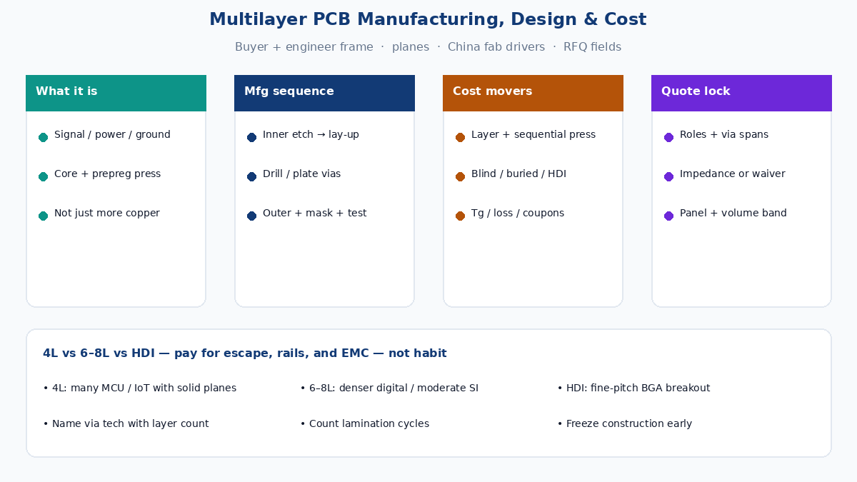
What multilayer means on the floor
A multilayer PCB is a pressed stack of copper foils and dielectric sheets. Outer copper usually carries pads, short breaks, and silkscreen real estate. Inner copper carries signal, power, and ground planes that only exist after inner imaging, etch, and lamination. Cores arrive as copper-clad laminate; prepreg is the resin-glass that flows and bonds under heat and pressure. The finished board is one rigid panel — but every buried net was once a separate etched sheet.
That is different in kind from a double-sided board. Two-layer work has no buried copper; every interlayer jump is a full-thickness plated through-hole. Multilayer work adds internal planes so return paths can sit next to continuous copper, power can spread on dedicated sheets, and routing density can rise without turning the top into a spaghetti pour. Signal integrity, power integrity, and EMI behavior become things you can plan — provided the construction matches what the press and plating line can hold.
Planes are not decoration. A solid ground next to a controlled-impedance net sets ohms with trace width and dielectric thickness. A fragmented pour two layers away invents a long return loop that shows up in the chamber, not in DRC. Power planes cut DC drop and give high-frequency bypass a low-inductance path when the stack puts them where decoupling needs them. Treat layer roles (signal / power / ground) as part of the fab contract, not as CAD labels you rename after placement.
Manufacturing sequence that explains the quote
China fab multilayer pricing makes more sense when you walk the panel the way the shop does.
Inner imaging and etch come first. Photoresist defines each inner copper layer; etch removes unwanted foil. Opens, shorts, and under/over-etch here become buried defects after press — expensive to find and hard to rework cleanly. More inner layers means more imaging cycles and more chance that one bad etch scrapes a whole sub-lot.
Lay-up and lamination stack cores and prepreg to the agreed construction, then press under heat and pressure. Alignment pins or optical registration keep layers from walking. Voids, resin starvation, and misregistration become warpage, thickness error, and delamination risk. Hybrid builds that mix resin systems need press recipes the fab has already proven — not a hope that "FR-4 plus RF laminate" will behave like a single-material menu.
Drilling and plating open vias and build conductive barrels. Mechanical drill after a single press is the baseline for through-hole multilayer. Blind, buried, and laser microvias usually need sequential build: cores or build-up layers are drilled and plated before the final press. Each extra sub-lamination cycle adds thermal stress, registration risk, and calendar time. That is why via technology often moves the quote more than adding one casual signal layer on a standard through-hole menu.
Outer pattern, mask, finish, and test close the path. Outer etch, solder mask, surface finish, electrical test, and — when specified — impedance coupons verify that dielectric and etch landed inside tolerance. Coupon language that does not match the drawing is a classic CAM EQ; waive impedance explicitly when you do not need it so quotes stay comparable.
General process primers cover etch-drill-plate at a high level. Multilayer cost lives in how many times the panel is cooked, how many via technologies share the traveler, and whether materials and coupons match the files.
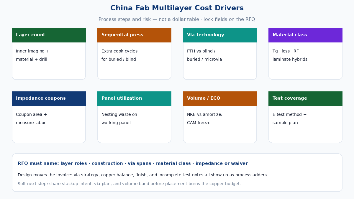
China fab cost drivers buyers under-specify
Layer count is the headline. It is rarely the whole invoice. Factories price risk and process steps:
| Driver | What the shop actually spends |
|---|---|
| Layer count | More inner imaging, more copper and dielectric, thicker stacks to drill/plate |
| Sequential lamination | Extra press cycles for buried/blind build-ups; yield and schedule risk |
| Blind / buried / microvia | Laser or controlled-depth drill, plating aspect ratio, extra registration |
| Material Tg or loss | High-Tg FR-4, low-loss or RF laminate vs commodity FR-4; moisture and press recipes |
| Impedance coupons | Dedicated coupon area, controlled etch, measurement labor; tighter % costs more |
| Panel utilization | Odd outlines, large keep-outs, or poor nesting waste panel area |
| Volume and change | Proto lots carry NRE and setup; frozen CAM at volume spreads tooling |
Layer count raises material and cycle time in a roughly stepwise way on standard through-hole menus. Jumping from four to six or eight on a stocked construction is often cheaper than staying at four while forcing blind vias and exotic dielectrics to fake density.
Sequential lamination is the quiet multiplier. Buried vias that force overlapping sub-laminations, or HDI build-ups that stack laser layers, cook the panel more times. Merging overlapping via structures into fewer cycles is often the manufacturable cost fix — not "add one more layer and hope."
Blind, buried, and microvia technology should be named the same day as layer count. "Blind/buried TBD" is how quotes diverge and how CAM later asks for a redesign after escape routing is frozen.
Material Tg and loss matter when reflow temperature, CAF risk, or RF loss budgets leave commodity FR-4. High-Tg grades cost more and may change drill and press windows. Low-loss or RF laminate hybrids cost more still and need CTE-aware press guidance. Do not name a brand on the RFQ unless that brand is a drawing requirement; call out Tg, Dk/Df targets, and whether a hybrid stack is allowed.
Impedance coupons are not free area. If controlled traces exist, put target ohms, reference layer, geometry, and tolerance on the drawing. If they do not, say so. Mixed language ("impedance if possible") produces mixed quotes.
Panel utilization is purchasing math. A board that nests poorly on a standard working panel pays for copper and process you never ship. Early outline and array talk with the fab beats discovering utilization after tooling.
Volume still matters. Proto and first-article carry CAM, tooling, and coupon setup. Production lots amortize those fixed costs — provided ECO churn does not reset the CAM clock every week.
Design choices that move the quote
Engineers control more of the invoice than a line-item "NRE" suggests.
Layer order and roles. Freeze signal / power / ground roles with the fab while the schematic is still movable. Late swaps that turn a stocked six-layer menu into a custom eight-layer hybrid after placement burn schedule and invite warpage EQs.
Via strategy. Default to through-hole when density allows. Reach for blind/buried or HDI when BGA pitch and escape force it — then count lamination cycles, not just via icons in the CAD library. Aspect ratio limits still apply: mechanical drills tolerate thicker stacks; laser microvias need thin outer dielectrics.
Copper weight and balance. Heavy copper on power layers raises etch and plating time and warps the stack if outer signal layers stay thin and unbalanced. Symmetry and copper balance are fab constraints, not aesthetics.
Trace/space and annular ring. Aggressive geometry that sits outside the fab's process capability class triggers either a no-quote or a yield adder. Match the drawing to a named capability class the shop already runs.
Finish and mask. ENIG, OSP, and immersion silver are not interchangeable on cost or shelf life. Mask dams, plugged vias, and selective finishes add process steps. Call them when needed; do not sprinkle them "just in case."
Test coverage. Flying probe vs fixture, netlist completeness, and impedance sample plans all show up as labor. Incomplete electrical test notes produce either padded quotes or weak acceptance.
None of this replaces a proper stackup drawing for impedance-critical work. It does stop treating multilayer design as "more layers = safer" without pricing the process behind those layers.
When 4L vs 6–8L vs HDI pays
Habit ("we always do six") and fear ("twelve looks safer") both waste money.
Four layers still pay for many MCU, IoT, and industrial I/O boards when one solid ground and one power (or dual ground) plane can carry return and PDN needs. If the product is connector-heavy but not BGA-dense, four-layer through-hole on a stocked menu often beats a casual six-layer with unfinished plane strategy.
Six to eight layers pay when denser digital routing, mixed-signal partitions, or moderate-speed interfaces need cleaner references without jumping to sequential HDI. USB 3.x, PCIe, and DDR-class links commonly land here when dedicated signal pairs want adjacent planes. Count rails and the largest package before counting "nice to have" signal sheets.
HDI (and higher sequential builds) pay when fine-pitch BGAs force laser microvia breakout, short stubs, and thin outer dielectrics that a single-press through-hole stack cannot deliver. HDI is not a prestige upgrade for every board. Each build-up layer is another press. If density does not require it, you are buying registration risk and calendar time.
A practical buyer check: ask whether the next layer (or the next via technology) removes a real escape, PDN, or EMC problem — or only comforts the layout review. Comfort is expensive on China fab travelers.
Odd layer counts press less evenly than even counts on most production menus. Specialty constructions exist; default even unless a real constraint forces otherwise.
RFQ fields for multilayer quotes that stay comparable
Market articles list "materials, volume, and complexity." Factories quote from fields. Put these on the RFQ or fab notes so apples stay apples:
| Field | Why it matters |
|---|---|
| Layer count and layer roles | Signal / power / ground names that match Gerbers |
| Construction | Core/prepreg types, dielectric thicknesses, copper weights, finished thickness ± tolerance |
| Via technology | PTH only vs blind/buried/microvia and which layers they connect |
| Lamination cycles | Single press vs sequential; do not leave "TBD" |
| Material | Tg, Dk/Df or loss class; hybrid allowed or not; RF laminate callouts if required |
| Impedance | Targets, references, geometry, tolerance — or explicit waiver |
| Impedance coupons | Required coupon count/location language |
| Outline and array | Panel utilization assumptions, scoring/V-cut, breakaway |
| Surface finish and mask | Finish type, thickness notes, plugged vias if any |
| Test | Continuity/isolation method, sample plan, microsection if Class-driven |
| Quantity and revisions | Proto vs production; ECO freeze point |
| File package | One revision of Gerbers or ODB++, drill, stackup notes, fab drawing |
If the RFQ only says "8-layer FR-4, impedance OK, blind vias maybe," expect either a padded quote or a CAM storm after award. Mirror the discipline you already use for copper weight and surface finish: name the process, not the hope.
For builds that live or die on reference planes and press sequence, keep a dedicated stackup discussion with CAM. This manufacturing-and-cost frame is the buyer companion to that work — not a substitute for freezing dielectric thickness and via spans on a drawing.
Soft next step
Start from the product constraints, not a layer-count habit. Count the largest package, the power rails, and which nets need controlled impedance next to solid planes. Choose the thinnest via technology that actually escapes the board. Put layer roles, construction, via types, material class, impedance (or waiver), panel notes, finish, and test on one RFQ package at one revision.
When those fields are clear, a China multilayer fab can quote process steps instead of guessing risk. Share the stackup intent, via plan, and volume band early — before placement burns the copper budget — and keep ECO churn off the traveler once CAM is frozen.