
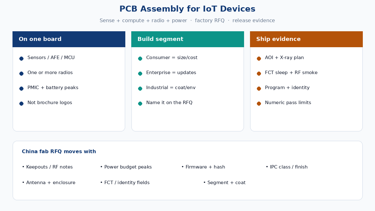
IoT products fail less often from "IoT strategy" than from a board that cannot sense, compute, radio, and power at the same time under the enclosure, battery, and factory test limits you actually ship. PCB assembly for IoT devices is that intersection: sensors and frontend analog, MCU or SoC, one or more radios, and a power tree that survives peak TX current — not a brochure list of Wi-Fi and Bluetooth logos.
This guide is for overseas engineers and sourcing teams quoting China fab / PCBA for connected products. It covers what "role of PCBA in IoT" means on a traveler, how consumer, enterprise, and industrial builds diverge, SMT density and battery power-domain budgeting, multi-radio coexistence keepouts and ground, module versus discrete antenna plus enclosure detune, AOI / X-ray / FCT / programming / identity, and a practical RFQ file checklist. Confirm stack, RF notes, and test limits with your fab drawing; do not treat market CAGR blurbs as engineering specs.
What "PCBA in IoT" actually means on the board
An IoT node is not a motherboard with a LAN jack bolted on. The assembled board is expected to:
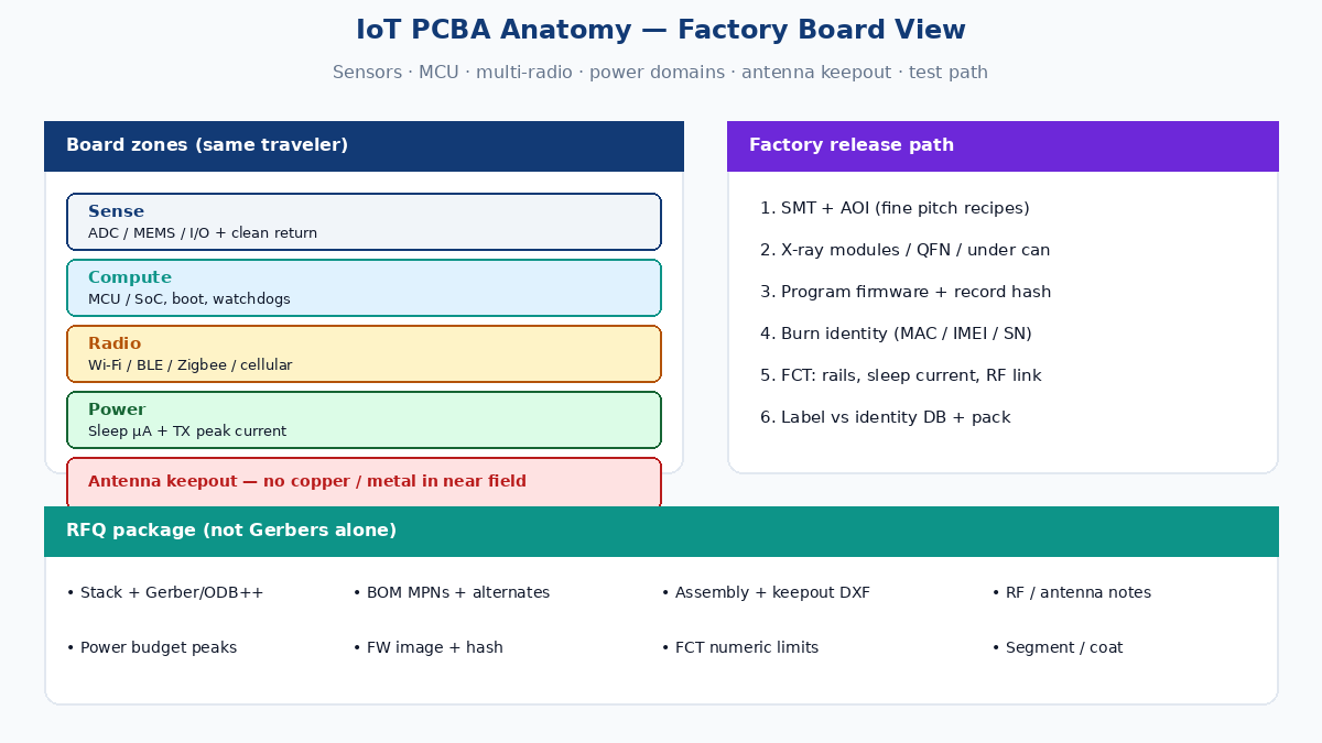
- Sense — ADC, AFE, MEMS, optical, or industrial I/O with clean analog return and filter layout that survives motor noise or LED PWM.
- Compute — MCU / SoC / module with boot, watchdogs, and firmware that must be programmed and verified in the factory, not only on a developer desk.
- Communicate — Wi-Fi, BLE, Zigbee / Thread, LoRa, cellular LTE-M / NB-IoT, or proprietary sub-GHz, often more than one radio on the same ground plane.
- Power — coin cell, Li-ion pack, USB, PoE, or 24 V industrial rail, with sleep currents in microamps and TX peaks that can be tens to hundreds of milliamps for milliseconds.
If any one of those four fails in production, the "smart" product is scrap or field returns. Brochure articles stop at sense / transform / communicate. Factory buyers need the fourth column — power domain budgeting — and the evidence path: AOI, X-ray where needed, functional test, RF smoke, and identity (MAC / IMEI / serial / keys) before the box ships.
Consumer vs enterprise vs industrial IoT builds
Same radios, different travelers.
Consumer wearables and home devices push thickness, cost, and battery life. Expect 0201 / 01005 where yield allows, module radios to shrink RF risk, plastic enclosures that detune PCB antennas, and ICT/FCT that must stay cheap at volume. Cosmetic AOI rejection rates and label accuracy matter as much as RF. IPC Class 2 is common; Class 3 is rare unless the brand mandates it.
Enterprise / commercial building (HVAC controllers, access, asset tags) adds longer duty cycles, denser connector sets, and firmware update paths that must not brick units already installed. Enclosure materials vary (metal housings kill PCB antennas). Buyers should name expected ambient, surge, and ESD class on the RFQ — not only "smart building."
Industrial IoT often means wider temperature, conformal coat or potting, higher vibration, and sometimes SIL / functional-safety adjacent process controls. Stack may stay FR-4 but copper weight, via strategy, and connector retention change. Test fixtures need nest design that survives oily floors. Do not assume a consumer BLE module layout ports cleanly onto a DIN-rail product with 24 V switching nearby.
Write the segment on the RFQ. A fab that quotes "IoT board, 4L FR-4, ENIG" without segment notes is guessing your keepouts, coat, and burn-in.
Segment also changes panelization and depanel. Consumer boards may use V-score for cheap breakaway; industrial boards with heavy connectors often need tab-route and fixtured break to protect RF cans and crystal packages. Ask the fab how they will handle boards with ceramic antennas near the outline — a cracked antenna after routing is an RF fail that AOI may never catch.
SMT density and battery power-domain budgeting
Miniaturization is real: SMT packs sensors, PMICs, and radios into footprints that through-hole eras could not. What brochure copy skips is partitioning power domains so sleep and TX do not fight.
Practical budgeting on IoT PCBA:
- Name the domains — always-on RTC / security, sensing, radio, actuators / LEDs. Each needs a rail or load switch you can gate.
- Quote peak, not average — BLE advertising and Wi-Fi TX peaks dominate battery IR drop and PMIC current limit. Coin-cell designs that only model average µA often brown-out on the first burst.
- Decoupling and return — radio PA and MCU digital share ground; star or partitioned returns reduce "random" packet loss that looks like firmware.
- Leakage killers — pull-ups left on during deep sleep, incorrectly biased FETs, and debug interfaces that stay powered. Factory FCT should measure sleep current with a hard limit, not a "looks OK" scope glance.
- Thermal — tiny boards with cellular or Wi-Fi modules dump heat into plastic. Thermal vias under modules and copper pours are part of the assembly drawing, not a late DFM surprise.
Density also drives inspection strategy: fine-pitch QFN / BGA under modules → X-ray sampling or 100% depending on risk class. AOI alone will not see voided pads under a shielded can.
On the BOM side, crystal load capacitance, RF matching tolerance, and battery connector plating are quiet cost drivers. Substituting a "same footprint" crystal without updating the load caps will shift BLE channels enough to fail association in a noisy factory. Lock alternates in writing; "or equivalent" without RF review is not equivalent.
Multi-radio coexistence: keepouts, ground, and clocks
Many IoT SKUs ship Wi-Fi + BLE, or BLE + Zigbee, or cellular + GNSS. Coexistence is not "pick three protocols from a list." It is layout and filter work:
- Antenna keepouts — copper-free zones, no ground pour under chip antennas unless the vendor drawing shows it, no tall metal (cans, screws, batteries) in the near field.
- Separation — distance between antennas, orthogonal polarization where possible, and notch filters or diplexers when sharing a path.
- Shared ground plane — unbroken reference under RF traces; slits for digital return that accidentally become slot antennas.
- Clock and spur control — switching regulators and MCU clocks that land on the radio band; spread-spectrum or layout distance helps more than another firmware retry.
- Shield cans — grounded properly to the plane; floating cans make emissions worse.
If your drawing has two radios and zero RF notes, China fab CAM will not invent coexistence for you. Put vendor antenna application notes and keepout DXF on the RFQ package.
For dual-radio boards, also document which radio owns the primary antenna and whether time-division or simultaneous TX is expected. Simultaneous Wi-Fi + BLE TX on a cramped wearable is a different coexistence problem than duty-cycled BLE with Wi-Fi mostly asleep. Firmware duty cycle belongs in the FCT script if you claim coexistence in the field.
Ground stitch vias along RF can edges, continuous pour under the RF section, and isolation of noisy motor driver returns from the RF return path are drawing items. CAM will not infer them from a marketing block diagram.
Module radio vs PCB / chip antenna — and enclosure detune
Two common paths:
Certified module (SiP or stamped metal can with onboard antenna or U.FL): faster FCC / CE path for many teams, higher BOM, still needs host PCB keepouts, ground clearance, and cable / enclosure rules. Programming and MAC provisioning still sit on your traveler.
Discrete SoC + PCB / ceramic / chip antenna: lower piece cost at volume, full RF responsibility on your layout and enclosure. Matching network, antenna feed length, and plastic dielectric constant become first-article killers.
Enclosure detune is where lab Wi-Fi RSSI dies in the molded product. Plastic thickness, paint with metal flake, battery under the antenna, and hand effect on wearables all shift resonance. Budget a tune pass with the production enclosure and the production battery — not an open-air FR-4 coupon alone. Soft next step for buyers: ask the fab/assembly house whether they can run a simple conducted or radiated smoke fixture against your golden unit after conformal coat / ultrasonic weld, not only before.
AOI, X-ray, FCT, programming, and identity
Brochure QC lists AOI and X-ray. IoT release needs more:
- AOI — polarity, missing parts, solder bridges on fine pitch; set recipes for dark components on dark mask.
- X-ray — BGA / LGA modules, QFN center pads, hidden joints under shields.
- ICT / flying probe — shorts, opens, basic analog; useful but not a substitute for radio bring-up.
- FCT — power rails, sleep current, sensor stimulation, button / LED paths, and a radio path: associate, ping, or AT-command loop against a known AP / gateway. Define pass/fail numbers (RSSI floor, current window), not "device connects."
- Programming / flashing — secure boot keys, firmware revision locked to traveler, checksum recorded. Partial flash that leaves factory test firmware in the field is a recall class event.
- Identity — serial, MAC, IMEI, certificates burned and logged against panel barcode. Cloud onboarding fails when identity is handwritten or duplicated across panels.
Industrial lots may add burn-in, coat thickness checks, and pair testing with a gateway golden sample. Put the evidence you need on the PO: which stations, sample rates, and what data returns with the shipment.
China fab / PCBA RFQ checklist (files and limits)
A usable IoT PCBA RFQ is not "Gerbers + BOM + 'IoT product.'" Send:
- Gerber / ODB++ / IPC-2581, stackup, impedance if any RF controlled lines, drill, and fabrication notes (finish, mask color, IPC class).
- Centroid / pick-place, BOM with MPNs (not only descriptions), approved alternates for passives and crystals.
- Assembly drawing — polarity, shield can locations, press-fit / connectors, coat keepouts, antenna keepout overlay.
- RF / antenna package — module datasheet keepouts, matching values, enclosure material note, cable lengths if U.FL.
- Power budget summary — sleep and peak TX currents, battery chemistry, expected FCT current limits.
- Firmware package — image, hash, programming adapter pinout, secure key handling instructions, version string for label.
- Test specification — AOI criteria, X-ray sample plan, FCT steps with numeric limits, identity fields to capture, packing / ESD notes.
- Segment / environment — consumer / enterprise / industrial, temperature, coat, vibration if relevant.
- Quantity and revision — prototype vs MP, ECO freeze date, first-article quantity and what "FAI pass" means (including RF).
Ask for a traveler outline back: which station owns programming vs FCT vs label. If the quote is only "SMT + AOI," you still own radio and identity risk.
Label and packing are part of IoT identity: anti-static bags with humidity cards where needed, MAC barcode readable after coat, and carton labels that match the identity database export. Field returns often start as "device cannot register" — which is an identity or firmware mismatch, not an SMT open.
When quoting multiple SKUs that share a PCB but differ only in firmware or radio enablement (Wi-Fi SKU vs BLE-only), say so. Partial stuff and DNP lists must appear on the assembly drawing; otherwise operators stuff every footprint and your sleep current fails FCT.
Soft next step
When you are ready to source an IoT board, package the files above and ask the China fab / PCBA partner for a first-article plan that includes sleep-current FCT, at least a basic RF association test, and identity capture — not only optical pass. That is how PCB assembly for IoT devices leaves the brochure and survives the field.