
Buyers who treat a soldered land grid array (LGA) like a ball grid array (BGA) with the balls “already there” usually discover the gap after first article: paste volume, pad geometry, and package/PCB flatness carry more of the joint than they expect. This page is a factory/buyer LGA guide for PCB pad design, solder paste, coplanarity, assembly inspection (including when X-ray still helps), and DFM/RFQ locks for China fab plus assembly — without inventing stock capability menus. Soft CTA only. Socketed CPU-style LGA is named where it matters; the manufacturing focus is directly soldered LGA. No competitor brands.
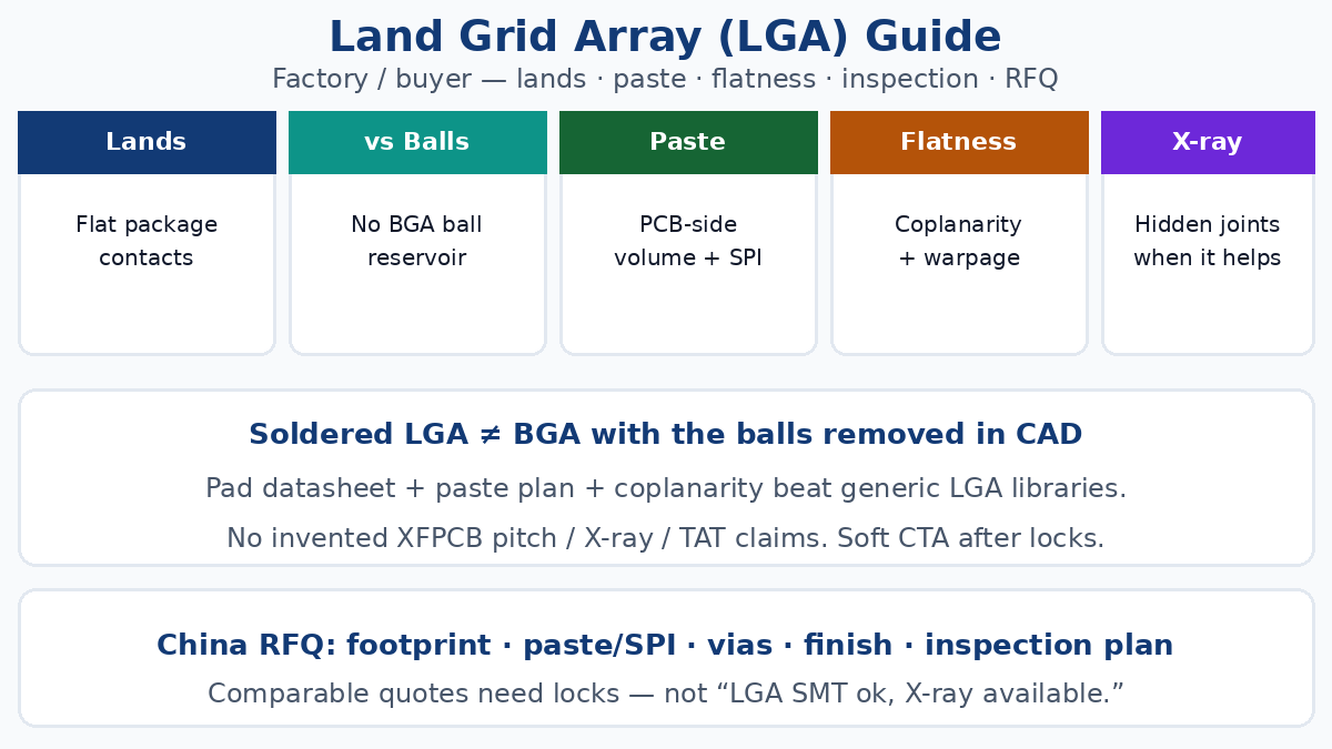
What a land grid array is on the board
An LGA package puts a grid of flat metal lands on the underside of the component instead of protruding pins or pre-attached solder balls. Electrical I/O still uses an area array — signal, power, and ground lands packed under the body — but the termination geometry is different from pin-grid or ball-grid packages.
Two board-level connection modes exist:
- Socketed LGA — lands press against spring contacts in a socket. Common for field-replaceable processors. The PCB sees a socket footprint, not a reflowed LGA joint field.
- Soldered LGA — lands wet to PCB pads through solder formed mainly from PCB-side paste during SMT reflow. After reflow, joints sit under the package body, hidden from ordinary optical view.
This guide assumes soldered LGA unless a paragraph says otherwise. Socket programs need mechanical and contact specs; soldered programs need paste, flatness, and hidden-joint inspection discipline.
LGA vs BGA for PCB and SMT buyers
Termination is the practical split:
| Topic | Soldered LGA | BGA |
|---|---|---|
| Package side | Flat lands | Pre-attached solder balls |
| Where most solder volume starts | Paste printed on PCB pads | Balls on the package (plus paste, depending on process) |
| Joint height / stand-off | Strongly paste + pad + coplanarity driven | Ball diameter and collapse dominate |
| Buyer pad risk | Undersize / wrong SMD vs NSMD vs datasheet | Escape, via-in-pad, mask, finish still critical |
| Hidden joints after reflow | Yes | Yes |
On a BGA PCB program, fab and CAM talk ball pitch, escape, via strategy, and mask openings that protect a ball-defined joint. On soldered LGA, the same shops still care about pitch and escape — but paste aperture volume and land-to-pad alignment become first-class yield knobs because there is no ball reservoir riding in with the part.
Do not copy a BGA stencil reduction onto an LGA footprint by habit. Ball processes and land processes are not interchangeable paste recipes. Lock the package datasheet land pattern and the assembler-approved stencil plan for that part number.
PGA (pin grid array) is the third cousin: pins into a socket or plated holes. LGA removes those pins; soldered LGA then inherits SMT hidden-joint problems rather than pin-bend problems.
PCB pad design that survives China DFM
Reliable soldered LGA starts with the component manufacturer’s recommended land pattern, not a generic “LGA pad” library entry.
Lock on the RFQ / fab note:
- Pitch and pad size from the package drawing (including any thermal / ground center lands)
- Solder-mask-defined (SMD) vs non-solder-mask-defined (NSMD) exactly as the datasheet calls — do not “improve” mask by local habit
- Solder mask opening and registration tolerance vs pitch (fine pitch leaves little room for mask shift)
- Surface finish compatible with wetting on small lands (call finish and any ENIG thickness expectation your PE already use)
- Via rules under or near lands — via-in-pad fill/cap, dog-bone escape, or keep-out — written so CAM does not invent a cheap via that steals solder into the barrel
Two LGA bodies with similar outlines can still need different pad sets. Treat the MPN land pattern as law; treat “we always use 0.X mm pads for LGA” as a clarifying question, not a process win.
Dense pitch often pushes escape into microvia / buried via territory. When the layout is truly high-density interconnect, say so and route the conversation through HDI PCB capability language (laser vias, sequential build-up, via-in-pad policy) instead of hoping a standard through-hole multilayer quote absorbs fine-pitch LGA fanout.
Thermal / ground lands. Large center pads need explicit paste coverage fraction, via pattern, and void expectations. Uncontrolled via wicking under a big thermal land is a classic void and open farm. Put thermal-pad paste and via notes on the assembly drawing, not only in a buried CAD property.
Paste, stencil, and SPI — the LGA volume problem
Because soldered LGA lands do not bring BGA-style balls, PCB-side solder paste largely sets joint volume and stand-off.
Buyer-level failure modes:
- Too little paste → opens, weak joints, extreme sensitivity to package tilt or PCB warp
- Too much paste → bridging, uneven collapse, solder smear toward neighbors
- Uneven paste height across the array → some lands wet; others kiss or miss
Stencil thickness, aperture size/shape, and paste release must follow the footprint and paste type — there is no universal “LGA stencil.” For fine-pitch or reliability builds, require 3D SPI before placement so volume, height, and offset get caught before reflow hides the evidence.
Ask the assembler to state (in the traveler or quote notes): stencil thickness class, aperture strategy relative to pad, paste alloy/type, and whether SPI is in-process or sample-only. “SMT included” without paste control language is not an LGA process lock.
Flatness, coplanarity, and warpage
LGA joints form where package lands, paste deposits, and PCB pads meet in Z. Coplanarity is the relationship among:
- Package land flatness / coplanarity spec
- PCB local flatness under the footprint
- Paste deposit height uniformity
- Placement attitude
- Dynamic warpage during reflow (package and board)
If one corner of the package sits high, lands there may never wet adequately even when SPI averages look fine. Opens that chase “add more paste” without checking warp can simply move the defect into bridges elsewhere.
RFQ gates that help:
- Package coplanarity / warpage notes from the MPN datasheet (buyer forwards; fab/assembler acknowledges)
- PCB thickness, stack symmetry, and any large copper imbalance near the LGA site
- Panelization and support strategy if the board is thin or heavily slotted
- Reflow profile ownership (paste vendor + component thermal limit + board mass) — no universal peak temperature claim
Warpage is a system problem. Paste-only fixes are incomplete.
Assembly flow buyers should recognize
A normal soldered LGA path inside PCB Assembly looks like:
Paste print → SPI (when required) → place → reflow → inspect → electrical / functional test
Placement accuracy tightens as pitch shrinks; the machine is aligning flat lands to pads without ball self-centering the way some BGA joints tolerate. Reflow follows paste and component limits plus board thermal mass — not a marketing “LGA profile.”
Lead-free vs tin-lead, nitrogen vs air, and soak/peak windows belong in the process card for the MPN, not as silent defaults on a mixed BOM.
Inspection: AOI, X-ray, and electrical — different jobs
After reflow, most LGA joints are under the package.
- AOI checks presence, polarity/marking where visible, gross placement, and other exposed defects. It does not see the full land-to-pad solder interface.
- X-ray is the usual tool for hidden joint shape: bridges, large voids, insufficient solder signatures, gross misalignment patterns. Use the live X-ray inspection lane when you need that method named on the PO — do not assume every quote includes it.
- Electrical test finds opens and shorts that the netlist can see. It does not prove void percentage or joint morphology.
When X-ray still helps even if the board “boots”: intermittent field returns, fine-pitch first articles, thermal-pad void concerns, process changes (new stencil, new paste lot, new fab lot), and any Class-style reliability expectation that cares about joint structure rather than “it powered once.”
When X-ray is not a substitute: wrong land pattern, chronic warp, or uncontrolled paste — imaging confirms symptoms; it does not rewrite the footprint. Pair methods; do not pick one checkbox and call the process closed.
Common soldered-LGA defect language (buyer table)
| Symptom | Typical contributors | Why buyers care |
|---|---|---|
| Open / insufficient | Low paste, poor release, non-wetting, coplanarity, warp | Field open, rework nightmare under package |
| Bridge | Excess paste, aperture/print offset, misplace | Hard short under body |
| Poor wetting | Oxidation, finish/paste mismatch, weak flux activity, bad profile | Marginal joints that pass room-temp electrical |
| Misalignment | Placement, datum, footprint mismatch | Partial lands, bridges |
| Voiding (esp. thermal pad) | Paste/outgas, via wicking, pad design, profile | Thermal and reliability risk if large / clustered |
Translate these into PO language: acceptance method (X-ray sample plan vs 100%, void criteria if you have one, SPI gates) rather than “good workmanship” alone.
DFM / RFQ locks for China fab + assembly
Send one coherent packet so fab and SMT quote the same part reality. Prefer structured Manufacturing Files plus assembly docs over a ZIP named final_final_3.
Minimum locks for soldered LGA programs:
- MPN and package drawing — land pattern, pitch, coplanarity/warpage notes, moisture sensitivity if relevant
- Gerbers / ODB++ / IPC-2581 with clear LGA pad and mask layers; stackup if impedance or thickness is controlled
- Assembly drawing — polarity, LGA site callouts, thermal-pad paste fraction, keep-outs
- Stencil / paste intent — thickness class, aperture notes, alloy; SPI requirement
- Via-in-pad / escape policy under the array
- Finish and cleanliness expectations that match fine-pitch wetting
- Inspection plan — AOI scope, X-ray yes/no and sample rule, ICT/FCT/flying-probe as applicable
- Quantity + first-article expectation — especially if paste/stencil will be tuned on FA
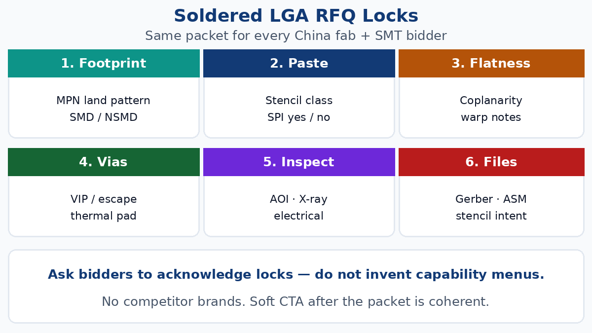
What not to invent on the RFQ. Do not claim a fab’s minimum pitch, X-ray machine model, or yield number you have not confirmed on a quote. Ask for acknowledgement of the locks above; let the bidder state process limits in their reply. Honesty beats brochure copy when customs paperwork and FA failures cost more than a clarifying email.
Quick-turn bare boards without SMT paste control are a different product than LGA PCBA. If you need both fab and assembly on a short clock, say so explicitly and keep the LGA process locks — speed does not erase coplanarity physics.
Soft close
Soldered LGA is an area-array SMT problem where lands + paste + flatness replace balls as the joint’s starting conditions. Lock the datasheet footprint, paste/SPI plan, warp awareness, and hidden-joint inspection method before competing China quotes on price alone. When your packet is ready, share Gerbers, MPN drawings, stencil intent, and inspection notes with XFPCB for a fab and/or assembly review — soft ask only; no capability theater required on either side.