
Industrial MCU control boards live next to 24 V cabinets, VFDs, relays, and field wiring — not on a USB-powered breadboard. When overseas buyers RFQ a China fab + PCBA line for that class of board, the failure modes are package inspection, placement against noisy power stages, input protection that survives surge and reverse polarity, isolation when grounds disagree, connector protection that matches the interface, and production programming / FCT language on the traveler. This note is the RFQ and DFM gate for that product: what “industrial MCU board” means versus a hobby or evaluation board, when MCU vs MPU changes layer count and impedance work, package → fab/assembly/inspection ladders, placement and power-entry practice, isolation and industrial interfaces, programming access, FCT fields, short finish/coat/IPC callouts, and a checklist that keeps CAM and assembly honest. It is not a chip-picker brochure and not a generic “industrial PCB standards” fluff piece.
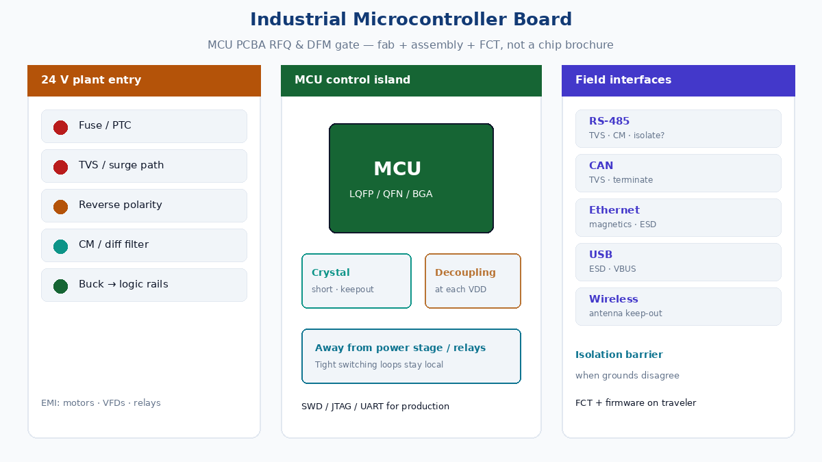
What an industrial MCU board is (and is not)
A hobby or development board is optimized for bringing pins out, USB power, and demo firmware. An industrial MCU control board is optimized for surviving the cabinet: continuous 24 V (or similar) plant voltage, motor and relay EMI, ground potential differences between panels, connector abuse, conformal coat or wash processes, and a production traveler that programs and functionally tests every unit.
Buyers who copy a Nucleo-style layout into a DIN-rail product usually discover the gap at NPI: no fuse or TVS path that matches the surge class, crystal next to a switching regulator, RS-485 without common-mode or TVS near the connector, SWD pads that assembly cannot reach after coat, and an RFQ that never named FCT or firmware load. Factory language starts from use environment and traveler, not from MCU part number marketing.
💡 Buyer check: Write the plant voltage, max ambient, coated vs uncoated, and whether field grounds can float relative to logic. Without those four, “industrial MCU PCBA” RFQs get hobbyist travelers with nicer silkscreen.
MCU vs MPU — when the PCB story changes
MCU boards (Flash + SRAM on-die, modest clocks, GPIO-heavy control) often stay on 2-layer or simple 4-layer FR-4 when speeds and EMI allow. The fab risk is mostly creepage around high-voltage or high-energy nets, solderability of the package, and assembly yield — not DDR routing.
MPU / application-processor style parts (external DDR, high-speed RGMII/PCIe-class interfaces, multi-GHz clocks in some SoCs) pull the design into 4+ layers, controlled impedance, length matching, and often HDI or fine BGA escape. That is a different RFQ: stackup notes, impedance coupons, and inspection for fine-pitch BGA become first-class fields.
| Board class | Typical stack pressure | When impedance / DDR enters |
|---|---|---|
| Simple industrial MCU (LQFP/QFN, ≤~100 MHz class clocks) | 2L often enough; 4L for EMI return and power | Rare — crystal and USB/Ethernet PHY may need local care |
| MCU + Ethernet / USB HS / multi-rail power | 4L common for solid returns | Local impedance for PHY pairs; confirm with fab |
| MPU + DDR + high-speed SerDes | 6–8L+ / HDI common | DDR and SerDes rules dominate stack and fab quotes |
Do not invent µm clearances or “we always do 2-layer for MCUs.” Layer count follows noise, voltage, and memory interface — confirm stack and impedance class with the fab before locking CAM.
Package → fab / assembly / inspection ladder
Package choice sets the inspection ladder more than the marketing pin count:
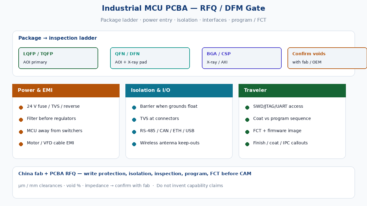
LQFP / TQFP. Leaded packages AOI can usually see. Wetting, bridging, and open heels are visible. Still call out lead finish and any form factor that fights paste print. Good default for many industrial MCUs when pin count fits.
QFN / DFN. Bottom thermal pad and perimeter lands. AOI sees the outer fillet; the center pad void and incomplete wetting often need X-ray or process capability evidence. Void criteria are confirm-with-fab / OEM — do not invent percent limits on the RFQ unless your standard requires them. Thermal vias under the pad need paste and via-fill notes so solder does not wick away.
BGA / CSP. Escape, via-in-pad policy, and X-ray (or AXI) become normal. AOI alone cannot prove joint integrity under the body. Pitch, ball count, and rework policy belong on the PCBA RFQ. CSP and fine-pitch BGA also tighten fab registration and solder-mask alignment.
Ladder language that travels: “LQFP → AOI primary; QFN center pad → X-ray sample or process window; BGA → X-ray / AXI per traveler.” Pair that with paste stencil thickness and any selective-solder or wave constraints for through-hole connectors still common on industrial boards.
Placement that survives motors and switching regulators
Placement is where industrial MCU boards either pass EMC/functional soak or bounce in the chamber.
MCU vs power stage / relays / switching regulators. Keep the MCU and its crystal/clock region away from relay coils, MOSFET/IGBT switching loops, and inductor fields. Return the switching loop tightly at the power stage; do not let that loop close through the MCU ground pour. Relays and contactors need coil snubbers and physical distance — a “short BOM” that drops the snubber shows up as MCU resets when the load clicks.
Crystal / oscillator. Short traces, grounded guard or keepout per the datasheet, away from switching edges and Ethernet magnetics. Do not park the crystal under a switching inductor or next to a 24 V connector that carries surge current.
Decoupling. Local ceramics at each MCU VDD/VSS pair; bulk where the datasheet and rail noise demand it. Industrial boards that “save” caps at the MCU while loading the same rail with a buck converter often chase phantom resets. Via to the plane at the pad when the stack supports it — confirm via size with fab, do not invent drill limits.
Analog vs digital islands. If the MCU mixes ADC and digital, keep sensor returns and digital return currents from sharing a long skinny neck. Star or partitioned returns beat a single noisy pour under everything.
24 V industrial input → logic rails
Plant voltage is rarely a clean bench PSU. A useful power-entry block for China PCBA RFQs names intent, not a secret schematic:
- Fuse or PTC sized for the fault energy you accept — location near the connector so a short does not cook the whole board.
- TVS / surge path for IEC-style or plant surge classes your product claims; return that clamp current to a robust chassis or input return, not through MCU ground pins.
- Reverse polarity diode or MOSFET ideal-diode — field wiring will reverse 24 V.
- Filter (common-mode choke, differential LC, or both) before regulators when VFDs and motors share the cabinet.
- Regulators (buck → LDO or multi-rail PMICs) with layout that keeps switching loops tight and keeps EMI off crystal and RS-485 PHY regions.
EMI from motors and VFDs couples through cables and ground. Shield and filter at the cable entry; do not expect the MCU decoupling alone to absorb cabinet noise. If the product claims a surge or EFT class, put that class on the RFQ so PCBA and test know what “pass” means — confirm exact levels with your compliance plan, not with invented factory defaults.
Isolation when field wiring disagrees on ground
Cabinets and remote sensors often sit at different ground potentials. Galvanic isolation (digital isolators, isolated DC-DC, optocouplers, isolated RS-485/CAN transceivers) is a layout and creepage problem, not only a BOM line:
- Keep primary / secondary clearances and creepage per the safety standard you claim; slotting and cutouts are confirm-with-fab geometry.
- Do not pour “helpful” copper across the isolation barrier.
- Route isolated interface PHYs so surge energy hits TVS and isolation first, MCU GPIO last.
- Name isolated supplies and grounds in net classes so CAM does not stitch them together.
Boards that skip isolation “because RS-485 is differential” still fail when one end’s ground sits tens of volts away from the other.
Interfaces — protection near connectors + test methods
Industrial MCU boards often mix several field buses. Protection and test belong next to the connector, not only in firmware.
| Interface | Near-connector protection (typical intent) | Test / FA notes |
|---|---|---|
| RS-485 | TVS / common-mode choke / failsafe bias; isolated transceiver when grounds float | Loopback or bit-error soak; common-mode stress if claimed |
| CAN | TVS, common-mode choke; bus termination policy | Bus load / error-frame checks in FCT |
| Ethernet | Magnetics, Bob-Smith / chassis strategy per design; ESD at magnetics | Link/speed bring-up; cable discharge awareness |
| USB | ESD array, VBUS protection; industrial use often gated or isolated | Enumerate in FCT; do not rely on host-only power in cabinet use |
| Wireless (Wi-Fi / BLE / LoRa modules) | Antenna keep-outs, ground clearance, metal enclosure detuning notes | RF functional check; shield can / coat keep-outs on RFQ |
Put TVS and filter parts on the PCBA BOM and placement notes. Buyers who leave “protection TBD” get bare connectors and field returns. Wireless modules need antenna keep-outs and coat/shield notes so conformal coat does not detune the antenna — confirm keep-out dimensions with the module vendor and fab, not with invented mm defaults.
Programming access for production
Prototype SWD pads under the MCU are useless after coat and enclosure. Production needs a deliberate path:
- SWD / JTAG header or pogo footprint reachable after assembly (and after coat if coat is applied before program — sequence matters).
- UART / bootloader pads if that is the volume programming path.
- Fixture notes: pogo force, alignment holes, and any boundary-scan if used.
- Security: readout protection and key provisioning belong in the process traveler, not as an afterthought silkscreen.
RFQ fields: programming interface type, fixture vs connector, pre-coat vs post-coat program, and firmware revision control. Silent “customer will flash later” boards create field mix of blank and half-programmed units.
FCT and firmware programming as PCBA RFQ fields
Functional circuit test and firmware load are PCBA line deliverables, not optional lab hobbies:
- Name FCT coverage at a useful level: power rails, digital IO sample, bus loopbacks, isolation withstand if required, and any sensor stim.
- Name firmware programming step: image hash, serial/UID write, calibration constants.
- State pass/fail logging and traceability if the OEM needs it.
- Separate ICT/flying-probe (assembly defect) from FCT (product behavior) so quotes do not confuse the two.
Boards that only specify “100% AOI” still ship with wrong firmware or dead PHYs. Put FCT + program on the RFQ even when ICT is also bought.
Finish, conformal coating, IPC class — short buyer callouts
Do not re-litigate full ENIG, coating chemistry, or IPC class articles here. For industrial MCU RFQs, state intent briefly:
- Finish — ENIG is common for fine-pitch and shelf life; HASL/LF-HASL still appears on thicker copper or cost-driven builds. Match finish to package pitch and press-fit if used; confirm with fab.
- Conformal coating — type (acrylic/urethane/silicone/parylene class), keep-outs (connectors, testpoints, RF antennas), and sequence vs programming. Coat over dirty flux creates leakage and adhesion fails.
- IPC class — Class 2 is common for many industrial controls; Class 3 only when the OEM contract truly requires it (tighter visual and performance criteria). Writing “Class 3” for a non-critical HMI board inflates cost without changing the field risk that actually matters (surge, isolation, FCT).
These are callouts, not substitutes for your finish/coat/IPC deep dives.
RFQ checklist for China fab + PCBA
Use this as a packing list before quote:
- Use environment: plant voltage, ambient, coated/uncoated, expected EMI neighbors (VFD/motor/relay).
- MCU vs MPU class and layer/stack intent; impedance only if Ethernet/USB-HS/DDR demand it.
- Package list with inspection ladder (AOI / X-ray / AXI).
- Placement notes: MCU–power distance, crystal keepout, decoupling intent.
- 24 V entry: fuse/TVS/reverse/filter/regulator intent and any surge/EFT class claimed.
- Isolation barriers and creepage notes where field grounds can differ.
- Interface protection near connectors (RS-485 / CAN / Ethernet / USB / wireless keep-outs).
- Programming access (SWD/JTAG/UART), coat vs program sequence.
- FCT scope + firmware programming + traceability.
- Finish, conformal coat type/keep-outs, IPC class as buyer callouts.
- Gerbers, BOM, centroid, stackup, and net-class notes that name isolated domains.
- Confirm µm/mm clearances, void %, and impedance targets with the fab — do not invent capability claims.
An industrial MCU board quote that only lists layer count and “STM32-compatible” is not an industrial RFQ. The traveler survives when protection, isolation, inspection, program, and FCT are written down before CAM starts.