
Buyers who type “HDI PCB advantages” usually already know the acronym. They need a sharper answer: which benefits are real on a China fab traveler, which applications actually force high-density interconnect, and which brochure claims fall apart once laser, fill, and sequential lamination show up on the quote. This page is the advantages-and-applications gate — not a density definition primer, not a stackup-and-DFM selection deep dive, and not an aerospace process-system page. Those jobs stay on their own drawings. Here the goal is buyer language: advantages you can tie to via architecture and layer-count tradeoffs, application gates that justify the process family, soft claims to refuse, and RFQ fields that lock the benefit so two shops are not quoting different boards under the same adjective.
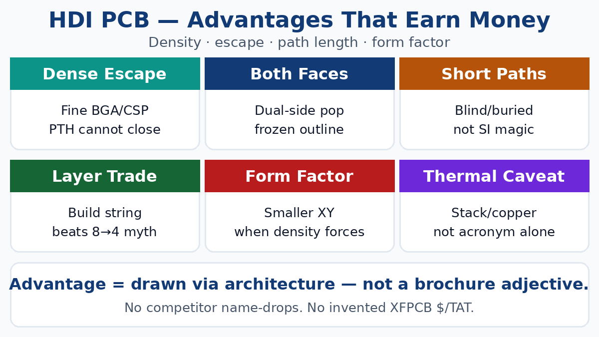
Advantages that earn money on a real traveler
Brochure lists often pile every positive adjective onto HDI: smaller, lighter, cooler, stronger, greener, always cheaper materials. Factory buyers do better when each claimed advantage maps to a structure or process step they can draw.
Higher component density on a frozen outline. Microvias, finer lines, and via-in-pad let both faces of the board carry dense packages without PTH dogbones eating escape channels. Dual-side population is not magic — it is a consequence of short interconnect and freed routing real estate. If outline can still grow a few millimeters, conventional multilayer may still win on cost.
Dense BGA / CSP / QFP escape that PTH cannot close. Fine-pitch balls choke through-hole fan-out. Blind microvias and filled via-in-pad (VIPPO-style language on the fab note) put interconnect under or beside the pads so mass-production escape stays honest. The advantage is reliability of the routing plan at volume — not a marketing claim that HDI “likes” BGAs.
Shorter interconnect paths. Blind and buried structures cut the vertical distance a net travels compared with a full-thickness PTH. Shorter paths can reduce loop inductance, crossing delay, and some crosstalk exposure when the stack and reference planes are designed for it. Signal integrity still needs models and controlled-impedance notes where required — HDI is not a free SI upgrade by acronym alone.
Layer-count and form-factor tradeoffs. A common industry illustration is replacing a thicker through-hole multilayer with a thinner HDI build that uses via-in-pad and one or two buildup levels — for example, an eight-layer PTH style plan that CAM can restate as a four-layer-class HDI skin when escape and impedance allow. Treat that as a design-specific trade study, not a universal recipe. Confirm build string (1+N+1, 2+N+2, or any-layer) on the stackup drawing; “HDI so we use fewer layers” without a traveler is how quotes diverge.
Mechanical and packaging outcomes. Smaller boards can mean lighter handheld products, less laminate area, and package envelopes that fit medical, wearables, or dense modules. Ruggedness claims need context: filled vias and fewer large perforations can help some mechanical stories; multi-lam registration and stacked-fill interfaces add other stress paths. Prefer drawn reliability arguments over “more solid because HDI.”
Thermal path caveats — not automatic heatsinks. Shorter copper paths can help heat leave a local hotspot faster in some layouts. Thermal expansion stress and life still depend on copper weights, dielectric Tg/CTE, via fill policy, and assembly reflow profile. Do not treat HDI as inherently higher heat resistance or as a substitute for copper pours, thermal vias called out on the drawing, or a metal-backed plan when power density demands it.
Power and battery narratives need honesty. Dense handhelds often ship with HDI because outline and BGA pitch force it; lower system power can follow from shorter nets and higher integration at the silicon level — not because laser vias magically cut milliwatts. Keep battery-life claims tied to the product architecture, not the fab adjective.
Soft claims to challenge before you buy the adjective
Thin advantage pages often over-promise. Push back in RFQ language:
- “Always cheaper materials.” Smaller XY can use less laminate, but laser stations, via fill/cap, LDI, and extra press cycles add cost and scrap risk. Unit price can go either way; compare travelers, not slogans.
- “Always faster prototypes.” Lead time tracks the shop’s HDI line load, material readiness, and revision freeze — not the word HDI. A conventional multilayer with stocked FR-4 can still ship sooner when density does not force lasers.
- “Inherently higher heat resistance.” Thermal behavior is stack- and copper-dependent. HDI without thermal design is not a heatsink.
- “More rugged by definition.” Stacked filled columns concentrate plating interfaces; staggered policies and proven fill/cap matter more than the marketing noun.
- “Sustainability of dense packages” as a blank check. HDI accommodates dense BGAs when via architecture and VIP policy are named. It does not forgive missing annular-ring, aspect-ratio, or fill notes.
If a benefit cannot be restated as a build type, via map, fill/cap line, or impedance note, it is brochure — not an RFQ advantage.
Applications: density gates, not prestige labels
Applications belong on this page as gates that force HDI, not as a gallery of industries that sound impressive.
Consumer handheld and wearables. Smartphones, compact IoT modules, and wearable PCBs often freeze outline while packing fine-pitch silicon. HDI earns money when escape and dual-side population are the only honest paths. If the enclosure still allows a larger PTH multilayer, skip prestige HDI.
Medical handheld and portable instruments. Density plus reliability paperwork (class, coupons, process control) often ride together. The advantage is fitting function into a clinician-friendly envelope — not a certificate claim invented on a blog. Name class/acceptance and via fill on the RFQ; do not imply device approval from fab process alone.
Industrial, networking, and compute modules. Dense connectors, multi-radio boards, and fine BGA controllers in compact housings hit the same escape wall. Prefer staggered microvias where life and multi-reflow matter; stack only where XY leaves no offset. Application language should still name build-up type.
Aerospace, defense, and high-reliability platforms. These programs may use HDI for weight and density, but the buyer gate is process system, class, and traveler discipline — not “military wants HDI.” Keep certificate and traveler depth on dedicated quality pages; here, only note that application prestige does not replace stacked-vs-staggered policy, fill/cap, and acceptance notes.
Automotive and harsh environments. Vibration, thermal cycling, and long life make fill quality, registration, and material notes first-class. HDI helps when module size and package pitch force it; environmental stress does not automatically select any-layer.
Across applications, the test is the same: if CAM can escape with conventional multilayer at acceptable size and layer count, HDI is optional. If annular rings starve, dogbones collide, or via-in-pad under fine balls is mandatory, name a build string and own the process cost.
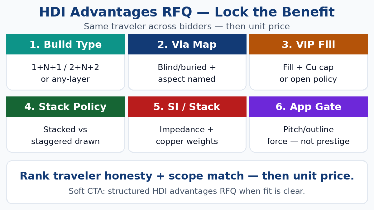
RFQ fields that lock the advantage (so quotes match)
Weak RFQs say “HDI for smaller board and better signal.” Strong RFQs make each claimed advantage checkable:
| Claimed advantage | RFQ lock so the shop cannot invent a quieter build |
|---|---|
| Dense BGA / CSP escape | Build-up type (1+N+1 / 2+N+2 / any-layer with N), blind/buried map, microvia diameter and aspect |
| Via-in-pad under fine balls | Via fill + copper cap (resin or conductive) named; open VIP policy stated if any |
| Shorter path / SI intent | Controlled-impedance nets and stackup reference where required; not “HDI so SI is fine” |
| Fewer layers / smaller outline | Stackup drawing with core vs buildup; layer count and copper weights outer / buildup / core |
| Stacked density vs reliability preference | Stacked vs staggered policy per region or net; mixed allowed if drawn |
| Thermal / life narrative | Materials notes (laser-drillable buildup family, Tg/CTE), class/acceptance, coupon or microsection expectations when density is high |
| Schedule honesty | Quantity, revision freeze, no silent build-type or VIP downgrade without signed EQ |
Compare bidders on the same table. Two “HDI advantages” quotes that omit fill/cap or build string are not comparable — one may be a single laser skin on a through-hole core; the other a multi-level SBU with VIPPO. Normalize the traveler before you rank unit price.
Impedance models, PDN plane strategy, and µm-level DFM bands belong on dedicated design pages. Here they appear only as locks that keep advantage claims honest on a China fab RFQ.
Soft next step
HDI PCB advantages that survive a buyer review are the ones you can draw: denser escape on a frozen outline, honest fine-pitch BGA routing, shorter interconnect where the stack supports it, and form-factor or layer-count tradeoffs confirmed on a named build string. Soft brochure claims — always cheaper, always faster, inherently cooler or tougher — need context or refusal. Applications justify HDI when pitch, outline, or via-in-pad force the process family; they do not justify it as prestige. Put build-up type, via aspect, fill/cap, stacked policy, impedance intent, materials notes, and class on the RFQ so every cited advantage maps to the same traveler. When the commercial fit is clear, send that structured package — XFPCB can respond on the field table without treating “HDI advantages” as a substitute for a frozen stackup and fab note.