
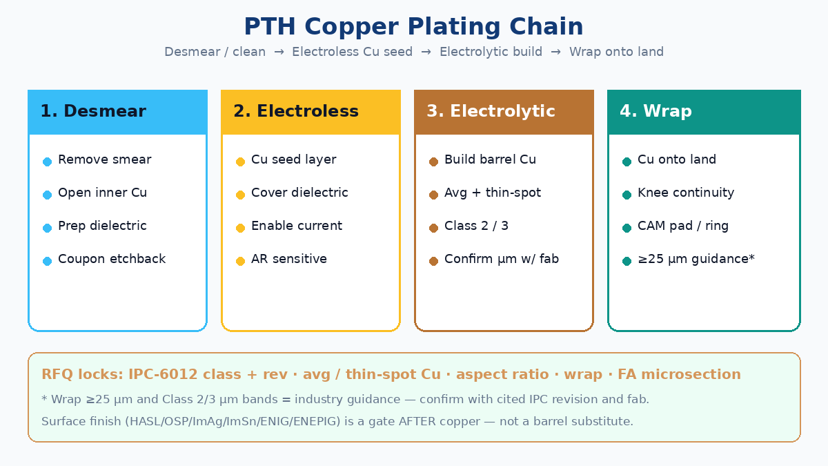
Through-hole copper plating is the chain that turns a drilled multilayer stack into a reliable barrel: desmear / clean → electroless copper seed → electrolytic copper build → wrap plating onto the land. Surface finish (HASL, OSP, ImAg, ImSn, ENIG, ENEPIG) sits after that copper work — it is a gate you choose once barrel and wrap meet the drawing, not a substitute for hole-wall thickness. Buyers who write “plate Class 3” with no average / thin-spot language, no aspect-ratio note, and no microsection plan get house defaults that pass continuity and fail life.
This China-fab guide answers first: the PTH plating traveler, what the RFQ must lock (Class 2 vs Class 3 copper language, aspect risk, coupon acceptance), why wrap plating matters to CAM, what inspection buyers actually ask for (microsection, XRF where relevant), and a finish-selection gate only — qualitative HASL / OSP / ImAg / ImSn / ENIG / ENEPIG. Deep ENIG black-pad and IPC-4552 thickness control belong in the existing ENIG surface-finish guide; this page does not rewrite that stack. Full fab flow and through-hole assembly (wave / selective / hole fill) are out of scope here.
Answer first: plating RFQ that survives CAM
| Buyer question | Factory / procurement answer |
|---|---|
| What is “PCB plating” on a multilayer fab PO? | Primarily PTH copper (seed + electrolytic build + wrap intent). Surface finish is a separate traveler step after copper |
| What must the RFQ lock? | Min average and thin-spot hole-wall Cu vs Class 2 / Class 3 language · aspect-ratio risk · microsection / coupon acceptance · wrap onto land |
| Why wrap plating? | Continuous copper from barrel onto pad/land improves via reliability; CAM sizes pads and mask so wrap can form and be inspected |
| How do you prove it? | Cross-section (microsection) on coupons or sacrificial holes; XRF for surface-finish metals where specified — not a replacement for barrel microsection |
| Finish gate? | Choose HASL / OSP / ImAg / ImSn / ENIG / ENEPIG by planarity, shelf life, pitch, and process risk — after copper specs are locked |
| Do not confuse with… | Through-hole assembly hole fill (IPC-A-610) · full “how boards are made” flow · ENIG black-pad deep dive |
💡 Procurement tip: Put bare-board class (IPC-6012 Class X, cite revision), PTH copper average + thin-spot intent, wrap language, and “FA microsection required” on the fab note and PO. “Good plating” is not measurable at receiving.
The PTH copper plating chain (traveler view)
After drill (and before outer-layer final pattern completion, depending on panel-plate vs pattern-plate flow), the hole wall must become conductive copper that survives thermal cycles. Factory sequence, compressed:
1. Desmear / clean
Drill leaves smear (resin) and debris on the hole wall. Desmear (chemical, plasma, or hybrid — process is plant-owned) opens interconnects to inner-layer copper and prepares dielectric for adhesion. Incomplete desmear → weak electroless nucleation, voids, or intermittent opens that electrical test may miss until thermal stress. Over-aggressive desmear can etch back glass or undercut inner copper — both show up on microsection, not on a continuity beep.
Buyers rarely write a desmear recipe. They do write acceptance: no smear bridging inner lands, no excessive etchback beyond the drawing / class window, and coupon evidence when Class 3 or high aspect-ratio holes are in play.
2. Electroless copper seed
Electroless Cu deposits a thin conductive seed on dielectric and on cleaned copper so electrolytic current can distribute into the barrel. Thin or patchy seed → thin spots after electrolytic build, especially in high aspect-ratio holes. RFQ language that helps: require process capability for your max aspect ratio (board thickness ÷ min finished hole), not a brand of chemistry.
3. Electrolytic copper build
Electrolytic plating grows the barrel copper to the specified average and minimum thicknesses. Panel vs pattern plate changes how outer and hole copper grow — do not invent a private process name unless you and the fab already agreed. Buyers own average and thin-spot barrel Cu, aspect-ratio flags, and coupon/microsection acceptance.
Industry guidance buyers commonly bring to EQ (always confirm with the fab against the IPC-6012 revision cited on your drawing — treat bands as conversation starters, not XFPCB capability claims):
| Acceptance theme (guidance) | Class 2 discussion band | Class 3 discussion band | Buyer lock |
|---|---|---|---|
| Average PTH Cu in barrel | Often discussed around ≥20 µm (~0.8 mil) class | Often discussed around ≥25 µm (~1.0 mil) class | Cite IPC-6012 class + revision; write average and how measured (microsection) |
| Thin-spot / minimum in barrel | Often a lower floor than Class 3 (commonly discussed near ≥18 µm class) | Often a higher thin-spot floor (commonly discussed near ≥20 µm class) | Explicit min thin-spot — average alone hides local starvation |
| Wrap onto land | Confirm class table in cited revision | Often discussed with wrap ≥25 µm (~1 mil) onto land as Class 3-style guidance | Wrap callout + pad geometry that allows wrap to form |
These µm/mil figures are IPC-class industry guidance to confirm — revision, hole type (PTH vs buried/blind), and plant capability all move the traveler. Do not paste brochure numbers as XFPCB promises.
4. Wrap plating intent
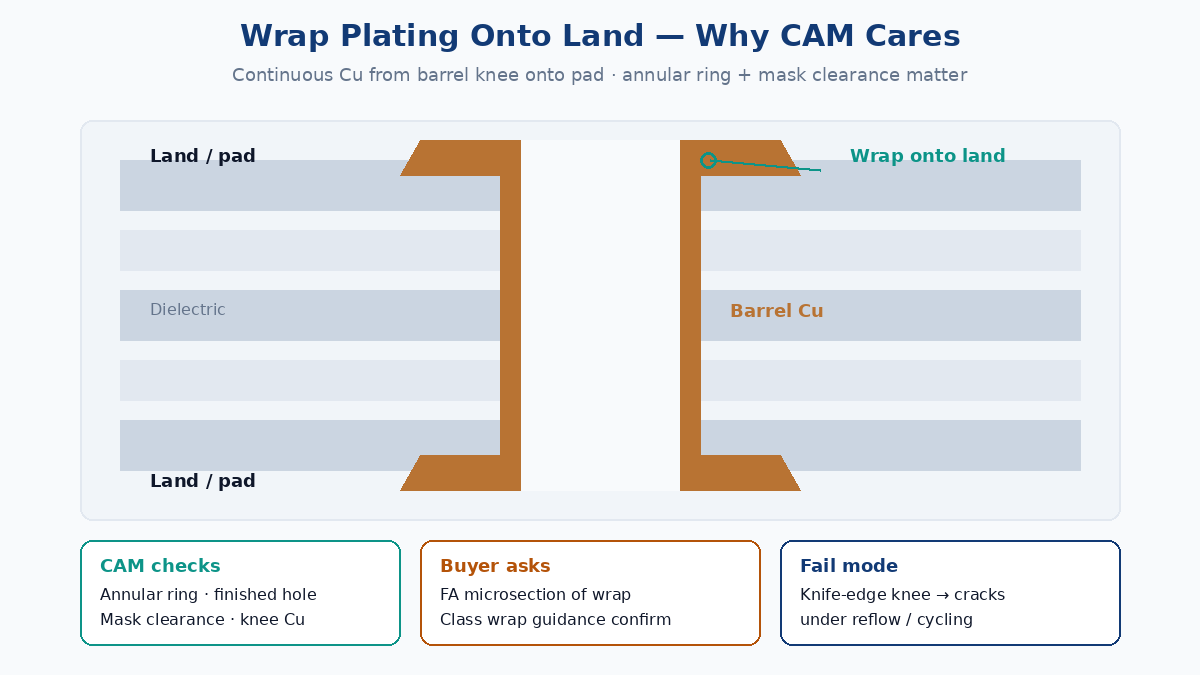
Wrap means electrolytic copper continues from the barrel onto the pad/land surface so the via is not a knife-edge transition at the knee. Weak wrap + thermal cycling → cracks at the land–barrel interface. That is why CAM cares about annular ring, pad diameter, solder-mask clearance, and finished hole size together — wrap needs copper real estate and a process window, not just a hope line on a PowerPoint.
What the RFQ must lock (Class 2 vs Class 3 language)
Vague “Class 3 plating” without numbers invites Class 2 economics and a debate after FA. Lock fields:
| RFQ / fab-note field | What to write | Fail mode if missing |
|---|---|---|
| Bare-board class | IPC-6012 Class 2 or Class 3 + revision | Plant defaults to commercial Class 2 windows |
| PTH Cu average | Min average hole-wall copper per class (confirm µm with fab / cited IPC) | “Looks plated” barrels with thin average |
| PTH Cu thin-spot | Min thin-spot / local minimum in barrel | Average passes; knee or mid-barrel starves |
| Aspect ratio | Max board thickness / min finished hole; flag high-AR holes | Quote assumes easy AR; scrap appears at plate |
| Wrap | Wrap onto land per class guidance (e.g. ≥25 µm as industry guidance to confirm) | Knife-edge knees; reliability arguments later |
| Microsection | FA coupon plan: which holes, layers, accept criteria | Verbal Class 3 with no cross-section evidence |
| No silent downgrade | No class / copper reduction without signed EQ | Traveler quietly reverts to thinner plate |
Aspect ratio risk (buyer view): Thick boards with small finished holes starve mid-barrel and knee copper first. If your stack is 2.4 mm with 0.25 mm finished holes, say so on day one. CAM will either stretch plate time, enlarge holes, or decline — all cheaper than field via cracks.
Class 2 vs Class 3 (practical): Class 3 buyers should expect longer plate, tighter thin-spot control, and coupon discipline. Class 2 is enough for many commercial boards when the drawing’s annular ring and copper floors match Class 2 and failure consequence is warranty-level. Do not “upgrade class” in an ECO without a DFM pass on pads and holes.
Why CAM cares about wrap plating
CAM does not plate by slogan. Wrap intent changes:
- Pad / annular ring — too little land after drill wander → wrap cannot meet Class 3-style floors even if the barrel average looks fine on a lucky coupon.
- Solder mask — mask tenting / damming that crowds the pad can complicate wrap inspection and surface-finish coverage on the land.
- Finished hole vs drill — oversize finished holes shrink remaining ring; undersize risks plate and assembly.
- Thermal reliability story — wrap and knee copper are where many via failures start under reflow and cycling.
Put wrap language next to annular-ring and class callouts so CAM flags pad growth before you freeze Gerbers.
Inspection: microsection, XRF, and what buyers ask for
Microsection (cross-section) — the barrel truth
Microsection is how you see average copper, thin spots, voids, smear/etchback, and wrap at the knee. Typical buyer asks:
- First-article coupons from the production panel (or agreed sacrificial locations)
- Photos / measurements of barrel Cu average and minimum, wrap onto land, and inner-layer interconnect quality
- Accept / reject against the cited IPC-6012 class and your fab notes
Electrical continuity alone does not prove Class 3 copper. A thin barrel can beep and still crack after reflow.
XRF — where it belongs
XRF (X-ray fluorescence) is the usual shop tool for surface-finish metal thickness (e.g. Ni/Au on ENIG, Sn on HASL/ImSn discussions) on defined pads. It is not a substitute for PTH barrel microsection. Buyers who ask “XRF the holes for copper” are mixing metrology families — correct the RFQ: microsection for barrel Cu; XRF for finish stack where the finish standard calls for it.
What else buyers reasonably request
| Ask | Purpose | Overreach to avoid |
|---|---|---|
| FA microsection report | Prove average / thin-spot / wrap | Demanding destructive section on every production panel without NRE |
| Process capability note for max AR | Confirm the plant plates your hole chart | Locking a private chemistry recipe |
| Lot CoC to stated class + copper notes | Traceability at audit | “Class 3 certified plant” marketing with no product callout |
| Finish XRF (when finish is ENIG/etc.) | Finish thickness evidence | Using finish XRF to claim barrel Cu compliance |
FQC and electrical test catch other defects — not thin copper. Keep those scopes separate on the PO.
Surface finish selection GATE (qualitative only)
Copper plating answers “will the via survive?” Surface finish answers “will pads wet and store?” Choose finish after PTH copper and wrap are locked. This table is a gate, not a rewrite of ENIG black-pad chemistry — for Ni/Au thickness, XRF windows, and black-pad bath control, use the existing ENIG surface-finish PCB guide.
| Finish | Planarity | Shelf / logistics | Pitch / use fit | Main process risk (qualitative) |
|---|---|---|---|---|
| HASL (SnPb or lead-free) | Uneven; poor for fine BGA | Modest | Coarse SMT, many TH boards | Coplanarity; skip for fine pitch |
| OSP | Flat | Short; handling sensitive | Cost-driven SMT, short pipeline | Multi-reflow / long storage |
| ImAg | Flat | Humidity / tarnish sensitive | Fine pitch when controlled | Creep corrosion / storage discipline |
| ImSn | Flat | Whisker / aging discussions | Fine pitch / press-fit contexts | Multiple reflow / aging windows |
| ENIG | Excellent | Long | Fine pitch, BGA, probe pads | Cost; black-pad if Ni/Au out of control |
| ENEPIG | Excellent | Long | Wire-bond + solder mixed needs | Cost; process complexity vs ENIG |
Selection rules that keep quotes comparable:
- Lock PTH copper / class / wrap first.
- Name one primary finish; if selective finish is needed, draw it.
- Do not invent %-premiums or XFPCB price deltas on the RFQ — compare finishes by planarity, shelf life, pitch, and risk.
- For ENIG depth (IPC-4552, XRF, black pad), stay on the ENIG guide; this page only gates the choice.
Fab-note block you can paste
Adapt numbers to the IPC revision you cite and confirm µm values with the fab before freezing:
Bare board: IPC-6012 Class [2/3] (rev [X]). PTH copper: min average and min thin-spot per Class [2/3] — confirm µm with fab against cited revision. Wrap plating onto land per class guidance (industry discussion often ≥25 µm for Class 3-style wrap — confirm). Max aspect ratio [thickness / min finished hole] as designed. FA microsection on coupons required; report barrel average, thin-spot, wrap, and interconnect. Surface finish: [HASL/OSP/ImAg/ImSn/ENIG/ENEPIG] — finish metrology per finish standard (e.g. XRF for ENIG). No class or copper reduction without signed EQ.
When that block sits beside the hole chart and stackup, China quotes price the same plating risk instead of racing on silent Class 2 defaults.
Related XFPCB guides (titles only)
- ENIG Surface Finish: IPC-4552 Thickness, Black Pad & vs HASL
- IPC Class 3 PCB Fabrication: Drawing Class, Coupons & RFQ
- How PCBs Are Made (full process overview)
- Through-Hole PCB Assembly Process (wave / selective / hole fill — assembly, not fab plating)
- FQC Final Quality Control & PCB Packaging
- Functional Circuit Testing (FCT)