
A glass substrate PCB is a circuit board built on a sheet-glass core (soda-lime, borosilicate, fused silica, alkali-free display glass, or other fab-qualified glass) with copper conductors formed on one or both faces. It is not FR-4 “woven glass cloth in epoxy,” not a transparent PET/PI flex film, and not a sintered ceramic (AlN / Al₂O₃) substrate. Buyers who write “glass PCB” without that distinction get quotes for the wrong family — or a polite decline after CAM opens the stack.
Use glass when the design actually needs what sheet glass can deliver: defined optical windows, X/Y dimensional stability under humidity and temperature that organic laminates struggle to hold, or selected RF / mmWave constructions where the fab has confirmed dielectric data for that glass type and thickness. Stay on FR-4, MCPCB, ceramic, or transparent polymer flex when those jobs are thermal dump, high via density, mechanical toughness, or see-through flex — not when marketing just likes the word “glass.”
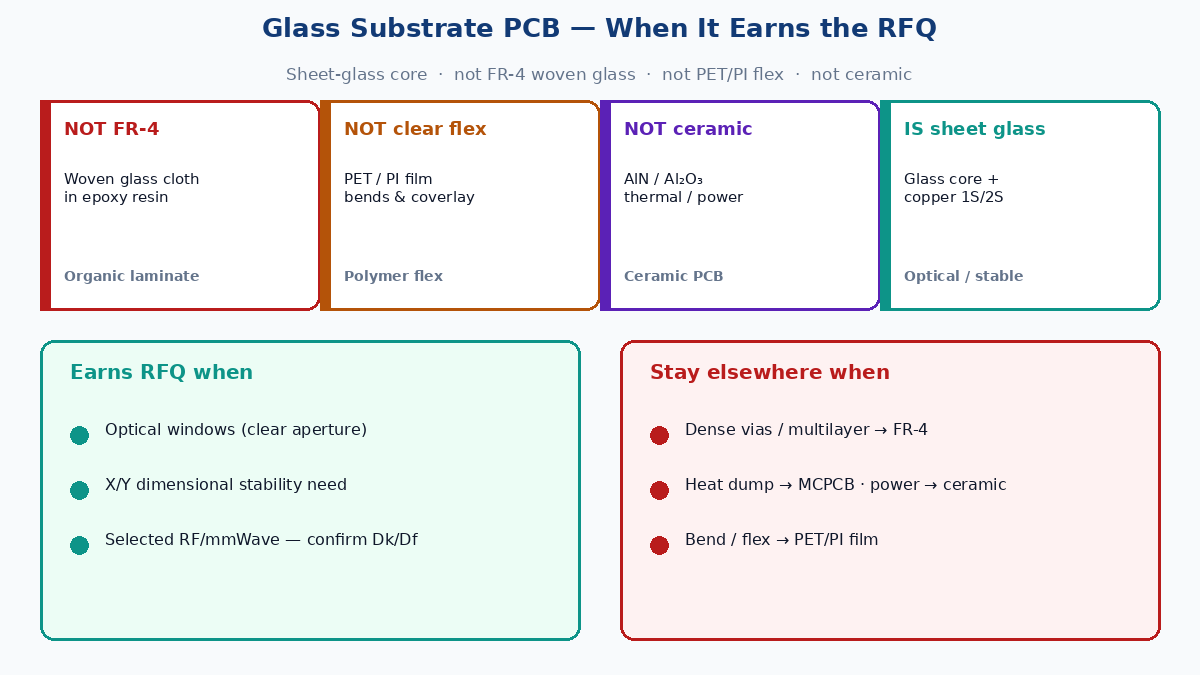
Answer first: when glass earns the RFQ
| Question | Factory / procurement answer |
|---|---|
| What is a glass substrate PCB? | Sheet-glass core + patterned copper (1S or 2S); optional plated holes. Dielectric = the glass sheet, not epoxy-glass cloth |
| What it is not | FR-4 laminate · transparent PET/PI flex · ceramic AlN/Al₂O₃ |
| When to RFQ glass | Optical windows through the board · dimensional stability beyond organic laminate · selected RF/mmWave after fab confirms Dk/Df for the exact glass |
| When not to | LED heat dump → MCPCB · high via / multilayer digital → FR-4/HDI · high thermal conductivity ceramic power → AlN/Al₂O₃ · see-through flex bends → PET/PI |
| Transparency reality | Copper, vias, mask, silk, and components kill full-board clarity. Spec optical windows, not “transparent PCB” |
| Biggest process risks | Brittleness · edge chip · drill/via difficulty · copper adhesion · SMT fixture / reflow handling · packing damage |
| 1S vs 2S | Double-sided + plated holes raise cost, scrap, and optical obstruction — call sides and hole intent on day one |
| RFQ minimum | Glass type + thickness · copper · holes · optical acceptance · finish · FAI photos · no silent glass swap |
💡 Procurement tip: Put glass family and thickness (mm), copper weight / process, hole map (NPTH vs plated), optical-window drawings, and “no substitute without EQ” on the RFQ. “Glass PCB, transparent” is not a traveler line.
Clarify the name — three things people confuse with glass PCB
1. FR-4 woven-glass laminate ≠ glass substrate
FR-4 (and most “FR-4 family” slash sheets) use woven glass cloth impregnated with epoxy (or similar resin). The reinforcement is glass fiber; the dielectric bulk behavior is resin + weave. Buyers say “glass epoxy” correctly for FR-4 — that still is not a continuous sheet-glass core with copper on glass.
If your drawing says glass but your intent is mid-Tg FR-4 stackup, stop and rewrite the material callout. You will waste a week and a NRE conversation otherwise.
2. Transparent PET / PI flex ≠ glass substrate
Clear or translucent PET and some polyimide flex constructions can look “glass-like” in photos. They bend, they take coverlay, they live in dynamic or static flex. Sheet glass does not flex like film. Optical flex and glass substrate are different RFQs, different tooling, different scrap modes.
3. Ceramic AlN / Al₂O₃ ≠ glass substrate
Ceramic PCBs (thick-film, DBC/AMB variants, etc.) are chosen mainly for thermal conductivity, high-temperature power, and ceramic CTE families — not for optical windows through soda-lime. Mixing “glass / ceramic / transparent” in one RFQ sentence is how three plants quote three incompatible processes.
When glass earns the RFQ
Optical windows (real reason #1)
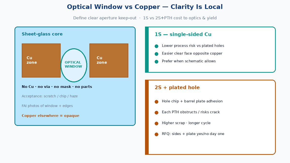
You need a clear aperture through the board for a sensor, LED/laser path, camera, barcode, or inspection beam — and the mechanical structure must still carry copper around that aperture. Glass can provide a flat, polishable, dimensionally stable window region if you keep copper, vias, mask, and components out of the optical zone and write acceptance (haze, scratch, chip, coating) in words CAM can inspect.
Do not assume the whole panel stays optically clear after fab. It will not if copper and finishes are present.
Dimensional stability (real reason #2)
Organic laminates move with moisture and reflow-scale heat. Sheet glass, for many display and borosilicate families, holds X/Y better in humidity-sensitive or alignment-critical assemblies (sensor arrays, optical benches, some precision interconnects). That is a mechanical / registration argument — confirm CTE and thickness with the fab for the exact glass; do not paste brochure ppm values into a purchase order without a datasheet revision lock.
Guidance bands buyers often bring to EQ (always confirm with fab for the glass you will actually buy):
| Property (guidance only) | Typical discussion band | What to lock |
|---|---|---|
| Sheet thickness | often ~0.3–1.1 mm class for small boards; thicker for mechanical; thinner for some display glass | Nominal mm + tolerance |
| CTE (in-plane) | glass families commonly discussed in low single-digit to ~tens ppm/°C depending on type | Named glass + datasheet rev |
| Dk @ RF | highly glass-dependent — do not invent | Measured or fab-supplied Dk/Df at your frequency |
| Surface | polished / as-drawn / coated | Ra or polish grade if optics matter |
Treat the table as conversation starters for EQ, not as XFPCB capability claims.
Selected RF / mmWave (real reason #3 — conditional)
Some glass types are discussed for low-loss or stable dielectric behavior at microwave / mmWave. Conditional: only after the fab (or a qualified materials lab) confirms dielectric constant and loss for that composition, thickness, copper process, and frequency. “Glass is good for RF” without numbers is marketing, not a stackup.
If your RF stack already works on a named low-loss organic laminate with handbook Dk/Df and a fab impedance coupon history, do not jump to glass for a slogan.
When to stay on FR-4 / MCPCB / ceramic / transparent polymer flex
| Need | Prefer | Why glass usually loses |
|---|---|---|
| Cost, multilayer digital, dense vias, BGA escape | FR-4 / HDI organic | Drill, PTH yield, multilayer process maturity |
| LED / power heat dump to metal | MCPCB (Al / Cu base) | Glass is a poor heat spreader vs metal core |
| High thermal conductivity ceramic power / RF ceramic | AlN or Al₂O₃ ceramic | Different process family; thermal is the ceramic story |
| Bend, fold, dynamic flex, ZIF | PET / PI flex | Glass cracks; flex films are designed to bend |
| “Looks transparent” for a demo photo | Often flex film + selective copper — or a windowed FR-4 with cutout + separate optic | Full-board glass clarity vs copper is a conflict |
| Drop / vibration / rough handling | FR-4 or ruggedized stacks | Glass edge and impact sensitivity |
Glass is a specialist substrate, not a drop-in upgrade for FR-4.
Transparency reality — define optical windows
Copper foil, plated vias, solder mask, legend, ENIG or other finishes, and every SMT part block or scatter light. A finished “glass PCB” with a full copper pour is about as see-through as any other board where the metal is.
Write the drawing like optics, not like a blog headline:
- Optical window region(s) — closed outlines on a mechanical or dedicated optical layer; keep-out for copper, mask, silk, and vias.
- Clear aperture size and positional tolerance to datum.
- Surface condition — which face is optical; polish / coating / AR if required (coating is often a separate process).
- Acceptance — scratch/dig or equivalent, chip size at edge of window, haze / contamination, photo method for FAI.
- Non-window areas — where copper and components are allowed.
If the product only needs a hole for a lens, a routed window in FR-4 plus a discrete optic may beat glass on cost and toughness. Glass earns the RFQ when the glass surface itself is the optic or the alignment plane.
Process risks China CAM will actually worry about
Brittleness and edge chip
Glass snaps. Panelization, V-score habits from FR-4, careless depaneling, and shipping without edge protection produce chips that become crack starters in reflow or drop test. Specify edge finish (as-cut, seamed, polished) and packing (foam, trays, no stacked bare edges).
Hole and via difficulty
Drilling or ablating glass is not the same as FR-4 carbide drill practice. Hole size, positional accuracy, chipping at entry/exit, and whether holes are NPTH or plated change tooling and yield. Microvias and high aspect plated holes are not “same as HDI FR-4.” Ask the fab what hole diameters and plating they will actually run on your thickness — do not paste FR-4 drill charts onto glass.
Copper adhesion
Copper on glass needs a qualified adhesion system (seed / adhesion layer / process of record). Peel strength and blister risk through reflow are process-owned. Call copper thickness (µm or oz equivalent as the fab quotes) and adhesion test method on the PO if reliability matters. Silent process swaps (different seed, different glass polish) are delamination tickets.
SMT fixture and reflow handling
Glass boards need support that FR-4 often skips: full-board fixtures, careful vacuum, controlled ramp, and operators who do not flex the panel “to check.” Warpage behavior differs from organic; localized heat can crack. Agree fixture ownership (fab vs assembler) before the SMT line scrap starts.
Pack and FAI photos
Require edge and window photos on first article. Cracks that hide under mask or at drill breakout show up late in the field. Pack notes belong on the traveler, not in a vague email.
1S vs 2S — and what plated holes cost you
| Construction | Typical use | Cost / yield / optics impact |
|---|---|---|
| 1S (single-sided copper) | Sensor windows, simple interconnect on one face | Lower process risk; one copper face; easier optical keep-out on opposite face |
| 2S no plate | Front/back patterns without interconnect | Alignment of two faces; still no barrel in glass |
| 2S + plated through-hole | True two-side interconnect | Highest difficulty: hole quality, plating adhesion in barrel, thermal stress; each plated hole is an optical and crack risk |
Plated holes buy electrical continuity and spend yield, cycle time, and clarity. If the schematic can live with edge connectors, conductive adhesive, anisotropic film, or one-side routing, say so on the RFQ — do not default to “PTH like FR-4.”
For RFQ comparison, force every bidder to state: sides of copper, plated yes/no, min hole, and whether optical windows remain free of plating stubs and mask bleed.
RFQ checklist — fields that stop silent swaps
Copy into the RFQ / drawing notes:
- Glass type — commercial name or composition family (e.g. borosilicate / alkali-free display glass / fused silica) + datasheet revision.
- Thickness — mm nominal and tolerance; panel vs finished part size.
- Copper — 1S or 2S; thickness (µm or oz as fab quotes); adhesion process of record.
- Holes — NPTH vs plated; diameters; count; plating thickness if plated; keep-out from optical edges.
- Optical acceptance — window drawings; scratch/contamination criteria; which faces are optical.
- Finish — ENIG, immersion silver, OSP, none on window, etc.; mask color and mask keep-out from windows.
- Outline / edge — cut method; edge chip criteria; scoring not assumed from FR-4.
- FAI — dimensional report + photos of edges, windows, and hole quality.
- No silent swap — any glass brand/type, thickness, seed/adhesion, or plating change requires written EQ before build.
- Assembly notes — fixture, max reflow profile assumptions, packing for ship-to-SMT.
Compare quotes only when those fields match. A cheaper line that omits glass type is not a bargain — it is an open material.
Factory closing
Glass substrate PCB is a named materials and process choice, not a synonym for FR-4 glass cloth, clear flex, or ceramic. It earns the RFQ when optical windows, dimensional stability, or fab-confirmed RF dielectric behavior are real requirements — and when the drawing respects brittleness, adhesion, holes, and the fact that copper kills clarity. Everything else stays on organic laminate, MCPCB, ceramic, or polymer flex.
Lock type, thickness, copper, holes, optical acceptance, finish, FAI photos, and no-swap language before CAM prices the job. That is how glass quotes stay comparable — and how first articles survive reflow and packing without a surprise crack.