

CAD shows a trace width. The fab ships a finished copper geometry. Those two numbers are related by etch factor, plating stack, artwork compensation, copper weight, and whether the layer is outer or inner—not by an IPC ampacity table. Overseas buyers who RFQ “min 4/4 mil, 1 oz, impedance OK” without freezing which width is controlled (drawn vs finished) and how differential pairs are biased get quotes that look identical and boards that do not.
This article is the geometry-control view for procurement and DFM sign-off. It is not a current-capacity catalog, not an impedance calculator tutorial, and not a rewrite of etch folklore. Deep etch-compensation and impedance-lock language live in PCB etch compensation for impedance geometry. Differential pair drawing needs live in differential pair routing. BGA fanout patterns live in BGA escape routing. Copper ounces as capability live in copper thickness capabilities. Here the question is: what RFQ and traveler fields freeze trace geometry so CAM, quotes, and FA measure the same thing—and which failure modes appear when those fields are missing?
Trace width is a process output
Finished trace width is what remains after:
- Base foil (and any foil treatment) on that layer
- Pattern definition (artwork, which may already be compensated)
- Etch undercut on the sidewalls
- On outer layers: pattern plate or panel plate copper that changes both thickness and lateral growth before or during etch, depending on the process flow
Inner layers are typically foil in / foil out with etch only. Outer layers see plating that interacts with the resist and etch chemistry. Treating “4 mil on L1” the same as “4 mil on L3” in the RFQ is how plants apply one compensation habit to two different process stacks.
Buyer implication: every critical width class on the drawing should state layer set (outer/inner), copper weight, and whether the dimension is finished or artwork. If you only state finished impedance targets, still freeze the fab’s compensation responsibility in writing—see the etch-compensation companion for the impedance-specific lock. This post freezes the commercial and DFM side: class, traps, neckdowns, pad exits.
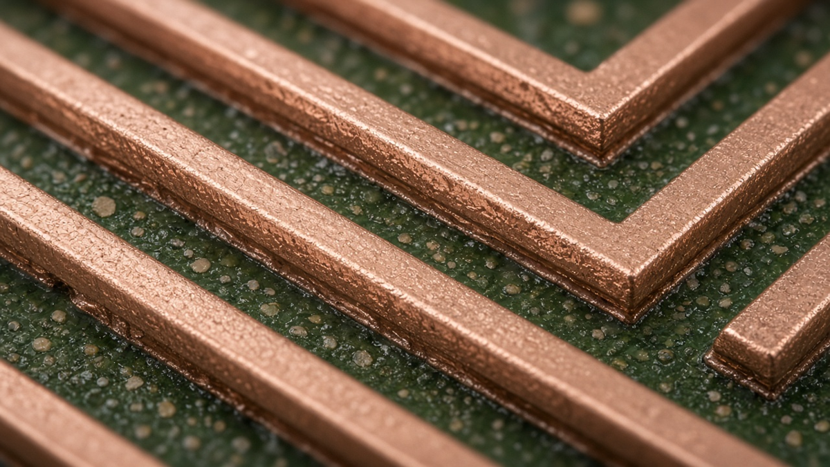
Drawn vs finished vs measured: three contracts in one word
| Term | Meaning | Who owns it | Fail mode if confused |
|---|---|---|---|
| Drawn / artwork width | Copper in Gerber before fab compensation | Designer or fab CAM (must say who) | Double compensation or none |
| Finished width | Copper after etch/plate as intended for SI or current | Shared; must be explicit on controlled nets | Impedance or neckdown surprise |
| Measured FA width | Microscope / coupon reading at agreed location | Quality vs drawing note | Arguments at FA with no method |
RFQ language that works: “Controlled impedance and min-trace callouts refer to finished geometry unless noted. Artwork compensation is fab responsibility per process; designer shall not pre-compensate unless stack note says otherwise.” Flip that rule only if your CAD library is already compensated for a named plant—and then name the plant and the library rev.
Outer vs inner: why the same mils are not the same risk
Inner layers
- Etch defines geometry from foil thickness; heavier foil generally means more undercut risk for the same drawn width.
- No outer plating growth, but thin cores and registration still matter for fine space.
- Heat and current behavior differ from outer (ampacity catalogs cover that elsewhere)—geometry risk here is mainly etch yield and clearance to copper pours.
Outer layers
- Plating adds copper; etch removes it. The finished width depends on the process sequence (PTH plate, pattern plate, etch) the plant actually runs.
- Solder mask openings and finish (ENIG, etc.) sit on the finished copper—mask-defined vs copper-defined pads change how traces leave pads (below).
- Fine outer lines next to large copper pours etch differently than isolated escapes—loading effects are real.
Quote trap: Plant A prices “4/4 mil outer 1 oz” assuming their standard compensation; Plant B assumes designer-compensated artwork. Same line item, different boards. Force both to restate compensation ownership and copper weight per layer class.
Min trace/space class is a capability claim—treat it like one
“Min 3/3” on a brochure is not your PO. Your PO needs:
- Minimum finished trace and space for the design’s worst net class (or “design uses X/Y finished; plant must support with margin”).
- Copper weight on those layers (copper thickness capabilities for what plants can run—not a substitute for stating oz on the stack).
- Outer vs inner separately if both have fine geometry.
- Coupon / FA measure expectation for the finest class if SI or yield risk is high.
- Whether HDI / specialty etch is required—or whether the design must stay inside commodity class.
Moving from commodity 5/5 or 4/4 finished into finer classes changes panel yield, inspection, and sometimes price break points. Cost-down that shrinks traces without shrinking the stated class on the RFQ is how you buy scrap.
| Buyer move | Why |
|---|---|
| State finished min trace/space used in the design | Stops “we support 3/3” quotes for a 5/5 board (and the reverse) |
| Split outer and inner mins | Different process risk |
| Tie copper oz to that class | Heavier copper + fine line is a different capability |
| Ban silent class upgrades | Plant should not “help” by etching finer without ECO if your library assumes commodity |
Copper weight vs etch factor: the quiet geometry tax
Heavier copper carries more current and raises finished thickness, but it also changes how much lateral etch you need to clear space. A design that barely clears 4 mil space at 1 oz may neck or bridge at 2 oz with the same artwork habit.
RFQ discipline:
- List copper weight per layer or per layer class, not one global “1 oz” when inners differ.
- If any layer is 2 oz+ with fine space, require the plant to confirm etch capability for that pair—or widen the class before award.
- Do not assume impedance models that used 1 oz foil still hold when purchasing swaps to 2 oz for “current margin” without re-locking width and dielectric.
This is a cost and yield decision as much as an electrical one: upgrading copper without revisiting trace/space is a classic respin trigger.
Differential pairs and etch bias (without rewriting pair tutorials)
Differential impedance cares about width and gap. Etch moves both. If compensation widens traces into the gap, Zdiff shifts even when “average width” looks fine.
Buyer callouts (details of routing rules stay in the differential pair guide):
- Pairs are finished geometry targets on named layers.
- Fab compensation must preserve pair intent (width and gap), not only single-ended width.
- Coupons for Zdiff on those layers; program to the stack rev.
- No one-sided etch bias “fixes” without updating both members of the pair.
Quote trap: single-ended impedance quoted; differential nets present; no pair coupon. Reject or add the row before award.
Failure modes geometry RFQs should anticipate
Undercut opens and mousebites
Excessive undercut on fine lines—especially with heavy foil or aggressive etch—leaves traces that look continuous to AOI at low magnification but open under thermal cycle or mild flex. FA cross-sections on the finest class catch this earlier than field returns.
Neckdown at BGA escape and pad exits
The drawn escape may meet min width in the field and still fail where the trace leaves a pad, via dog-bone, or teardrop is missing. Acute exits and mask ridges create etch and assembly stress concentrators. BGA fanout pattern choice belongs in the escape guide; the RFQ note here is: worst-case finished width includes pad exits and necks, not only mid-span track.
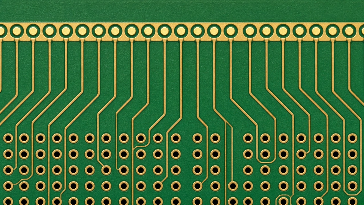
Solder-mask-defined vs copper-defined pads vs trace exits
- Copper-defined pads: mask opens larger than copper; trace exit is mostly a copper geometry problem (etch + clearance).
- Solder-mask-defined pads: mask opening defines the land; copper may be larger underneath. Trace exits under mask ridges can see different etch and soldering behavior; tented or tight mask dams near fine escapes amplify issues.
Call out pad definition style for fine-pitch and BGA on the drawing. Mixing styles without notes produces CAM defaults that fight your library.
Space erosion to pours and planes
Pour clearance equals space class in practice. A “4 mil space” design with 3.5 mil pour clearance after compensation is a bridge lottery. Freeze pour clearance ≥ finished space class (or state an intentional exception).
Repair and scrap economics
Fine-line opens on inner layers are often scrap, not repair. When you push class for density, price the scrap risk into the vendor choice—not only the unit panel price.
Quote traps checklist (geometry edition)
| Trap | What the quote hides | What to require |
|---|---|---|
| Brochure min without design min | Capability theater | Design’s finished min + margin |
| One compensation assumption unspoken | Artwork vs finished mismatch | Written compensation owner |
| Global 1 oz with mixed layers | Wrong etch/impedance | Per-layer or class copper |
| Outer fine line priced as inner | Process underbid | Outer/inner split |
| Impedance without geometry freeze | Dk-only theater | Finished width/gap + coupon |
| Diff pairs as single-ended | Gap ignored | Zdiff + pair coupon |
| Class shrink after award | Silent density creep | ECO to change min class |
| “We’ll CAM fix necks” | Uncontrolled artwork edits | Modification report + approval |
RFQ / PO geometry freeze block
Paste and require bidders to mirror:
| Field | Freeze |
|---|---|
| Geometry basis | Finished vs artwork; who compensates |
| Min finished trace/space | By outer and by inner (values your design uses) |
| Copper weight | Per layer / class; heavy-copper fine-line confirmation |
| Controlled impedance nets | Layers, targets, finished geometry responsibility (impedance control process as applicable) |
| Differential pairs | Present Y/N; Zdiff; coupon |
| Pad definition | SMD / CMD callouts on fine pitch / BGA |
| Neck/exit rule | Worst-case width includes exits; teardrops Y/N policy |
| Pour clearance | ≥ space class or listed exceptions |
| FA measure | Finest class locations / coupons required Y/N |
| CAM edits | No silent width/gap changes; report + approve |
| Class change | ECO only |
A quote that cannot restate compensation owner and outer/inner mins is not ready for fine geometry—even if the price is attractive.
How this sits next to etch-compensation and stack locks
- Stack / dielectric lock sets the vertical recipe for impedance.
- Etch-compensation lock sets how artwork becomes finished width for SI.
- This geometry freeze sets the commercial class, copper pairing, neck/pad rules, and quote comparability for all critical traces—not only impedance nets.
Use all three on boards that mix power necks, BGA escapes, and controlled pairs. Skipping the freeze and only locking Dk is how “impedance passed coupon” coexists with open escapes on the product.
Stage note for proto vs volume
Prototype spins may temporarily run looser class with flying-probe learning. Before ramp, freeze the geometry block to the revision you will tool. Changing min class or copper weight after stencil and ICT pads exist is an ECO cluster—not a free CAM tweak.
Decision worksheet before the next Gerber drop
- What is the finest finished trace/space actually in the design—outer and inner separately?
- Who compensates artwork—fab default or your library—and is that written?
- Does any fine class sit on heavy copper? If yes, is capability confirmed or class widened?
- Are differential gaps part of the controlled geometry, with coupons?
- Do BGA/pad exits meet the same finished min as mid-span, with pad definition called out?
- Does the RFQ freeze block appear on the quote line-by-line?
- What fails first if etch drifts—open, bridge, Z shift, or neck burnout—and is FA aimed there?
Answer those in the traveler. Ampacity calculators size current; they do not freeze fab geometry. A trace geometry RFQ freeze—compensation owner, class, copper pairing, necks, and pad exits—does. When density or copper weight changes, reopen the freeze on purpose; do not inherit last board’s 4/4 assumption onto a new escape map.