
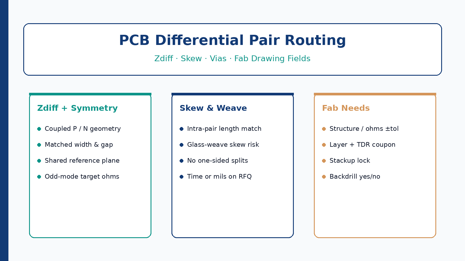
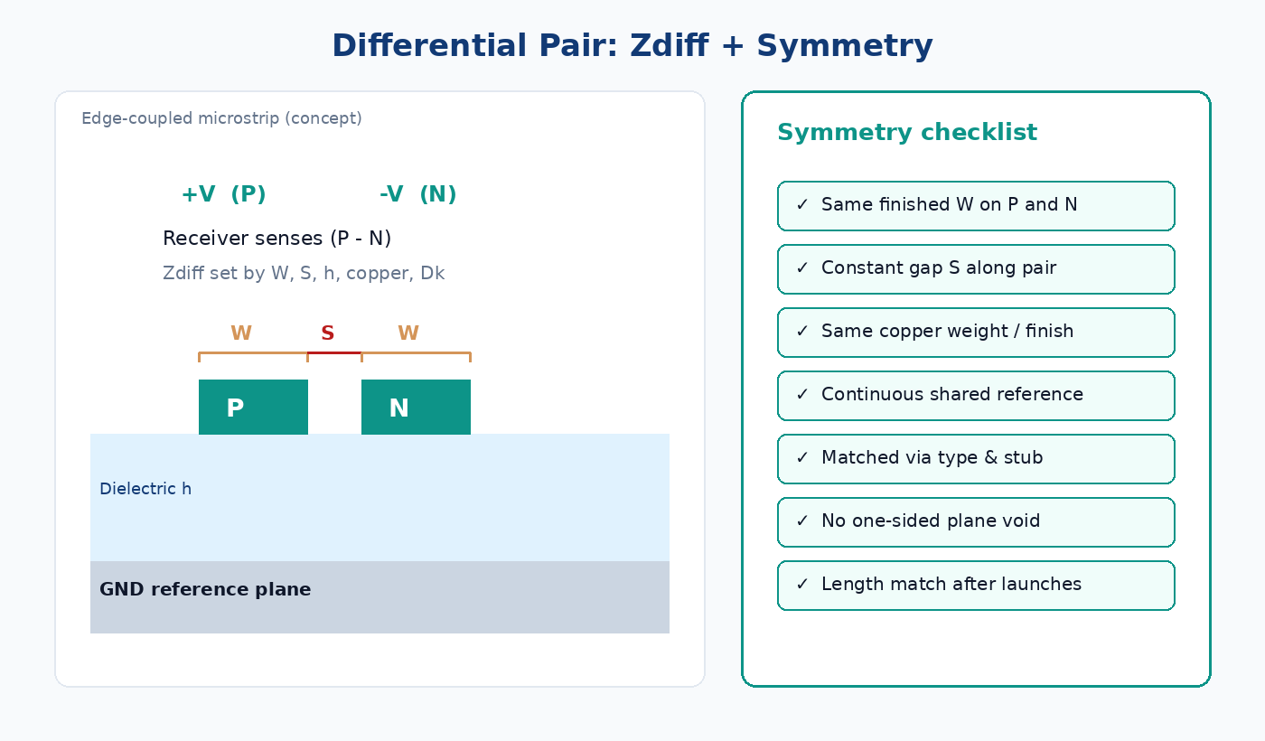
A differential pair is two tightly coupled traces that carry equal-and-opposite signals so the receiver looks at the difference, not the absolute voltage on either line. What fabs actually control is differential impedance (Zdiff), within-pair length match (skew), and reference-plane continuity — not the CAD “diff pair” net name alone. Symmetry matters because any mismatch in width, spacing, copper weight, dielectric height, or via stub turns common-mode noise into bit errors on USB, PCIe, HDMI, and similar links.
This page answers first for China PCB buyers and layout owners: what Zdiff targets mean on a fab drawing, how etch compensation and finished copper fool CAD widths, when glass-weave skew is a real RFQ issue, when backdrill or microvia enters the quote, and which fields make a controlled-impedance RFQ comparable across plants.
Answer first: what a diff pair is and why Zdiff + symmetry matter
| Idea | Factory meaning | Buyer trap |
|---|---|---|
| Differential pair | Two traces routed as a coupled structure with a defined Zdiff | Treating any two parallel nets as “controlled impedance” without a stackup lock |
| Zdiff | Impedance of the odd-mode / differential mode the fab will TDR | Quoting “90 Ω USB” with no layer, structure, or tolerance |
| Symmetry | Matched width, gap, copper, dielectric, and via transitions within the pair | Matching total length while one side hops layers or crosses a split |
| Length match / skew | Intra-pair delay match (ps or mils) after fab etch | Specifying mils without stating which CAD layer or netlist rule wins |
| Reference | Continuous GND (or defined return) under the pair | Crossing a plane split or void under one leg only |
Common protocol targets (confirm on the IC datasheet and PHY guide — these are starting points, not universal law):
| Interface (typical) | Zdiff target | Notes for RFQ |
|---|---|---|
| USB 2.0 HS | ~90 Ω | Often microstrip on outer; keep stubs short at connector |
| USB 3.x / USB4 lanes | ~90 Ω | Stub and weave skew matter more as rate rises |
| HDMI | ~100 Ω | Check sink/source and cable-side rules |
| PCIe | ~85 Ω (common) | Confirm generation; backdrill often appears on thicker boards |
| Ethernet (100Ω diff) | ~100 Ω | Magnetics and connector pinout drive via strategy |
💡 Procurement Pro-Tip: Put structure + ohms ±tol + layer + coupon on the fab drawing before you ask for price. “Impedance control yes” without those four fields is how one plant quotes FR-4 ±10% microstrip and another quotes hybrid material ±5% stripline against the same Gerber set.
Related stackup and material context: controlled impedance custom PCBs and PCB dielectric constant & dissipation factor.
Fab drawing impedance table: the format that unlocks real quotes
China fabs price and process controlled impedance from the drawing table, not from a Slack message. Give them a row per structure:
| Field | Example | Why it matters |
|---|---|---|
| Structure name | DP_USB_L1, DP_PCIE_L3 | Unique ID for DFM and TDR report mapping |
| Type | Edge-coupled microstrip / stripline / broadside | Changes etch, dielectric, and coupon design |
| Zdiff | 90 Ω ±10% (or ±5%) | Tolerance drives material and process cost |
| Single-ended Zo (if needed) | 50 Ω ±10% | Some stacks mix SE and diff on same layers |
| Layer | L1 (ref L2), L3 (ref L2/L4) | Locks dielectric height and copper weight |
| Trace / space (finished intent) | 5.0 / 5.0 mil finished | State finished vs artwork — see etch trap below |
| Copper weight | 0.5 oz / 1 oz finished | Finished copper changes Zdiff more than CAD often shows |
| Coupon | On-board TDR coupon required | No coupon = unverifiable “impedance OK” verbal |
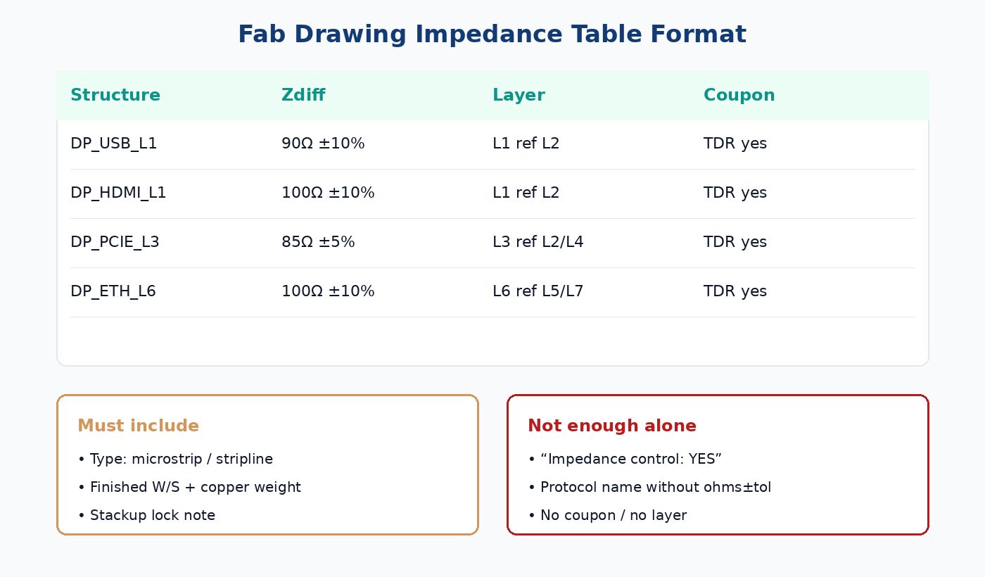
Also mark on the drawing: do not adjust stackup without written approval; list laminate family (or “fab may propose equivalent Dk with customer lock”); and require impedance report with serial/lot linkage.
For DDR-style length rules that sit next to high-speed diff pairs on the same board, see DDR PCB layout guide. Broader layout hygiene: PCB board design & layout considerations.
Etch compensation and finished copper vs CAD width traps
CAM will often compensate artwork so the finished line width hits the impedance model. Buyers get burned in three ways:
- CAD width ≠ finished width. You draw 4.5 mil; fab etches from 5.2 mil film to land at ~4.5 mil finished. If your RFQ says “do not change Gerber” but also “hit 90 Ω,” the plant must either refuse or violate one instruction — clarify which wins.
- Finished copper weight. Plating on outer layers thickens traces and narrows gaps. Outer microstrip Zdiff drifts if the stackup assumes 0.5 oz finished but the traveler runs 1 oz.
- Mask and plating. Soldermask thickness and ENIG vs OSP change outer Zdiff slightly; for ±5% jobs, ask the fab which finish the coupon assumes.
| Trap | What to write on RFQ / drawing | What not to do |
|---|---|---|
| Artwork vs finished | “Impedance to finished geometry; fab may compensate artwork within DFM” or “no compensation — buyer owns Zdiff risk” | Silence on who owns compensation |
| Copper | “Finished copper weight per layer in stackup table” | Only listing “1 oz foil” without finished callout |
| Gap under mask | Confirm soldermask over pair yes/no for Zdiff model | Assuming LPI has zero effect on ±5% outer pairs |
⚠️ Factory callout: If two China fabs quote wildly different unit prices on the same “90 Ω” board, compare (a) tolerance ±10% vs ±5%, (b) locked stackup vs “fab choose,” and (c) whether TDR coupons are included. Those three lines explain most of the delta.
Glass weave and within-pair skew: buyer-practical note
Glass weave (fiber glass style in the laminate) creates local Dk variation. On long, tightly spaced pairs at multi-Gbps rates, one leg can sit over more resin and the other over more glass — within-pair skew that length matching in CAD cannot fully erase.
Practical buyer rules (not a full SI treatise):
- For USB2 / many HDMI consumer runs on short boards, standard FR-4 weave is often acceptable if length match and Zdiff are controlled.
- For PCIe Gen3+, USB3.x long routes, and anything where the PHY eye is already thin, ask the fab about spread-glass / flat-weave options or rotate the pair relative to weave (layout) — and put the material note in the RFQ so both bidders price the same laminate class.
- Spec skew in time (e.g. ≤5 ps) or mils and state the max route length class so DFM knows whether weave mitigation is in scope.
Do not pay for exotic weave on a 50 mm USB2 pair “because the checklist said so.” Do escalate weave when the same checklist shows multi-inch PCIe lanes on FR-4 with ±5% Zdiff and backdrill.
Via stubs: when backdrill and microvia enter the quote
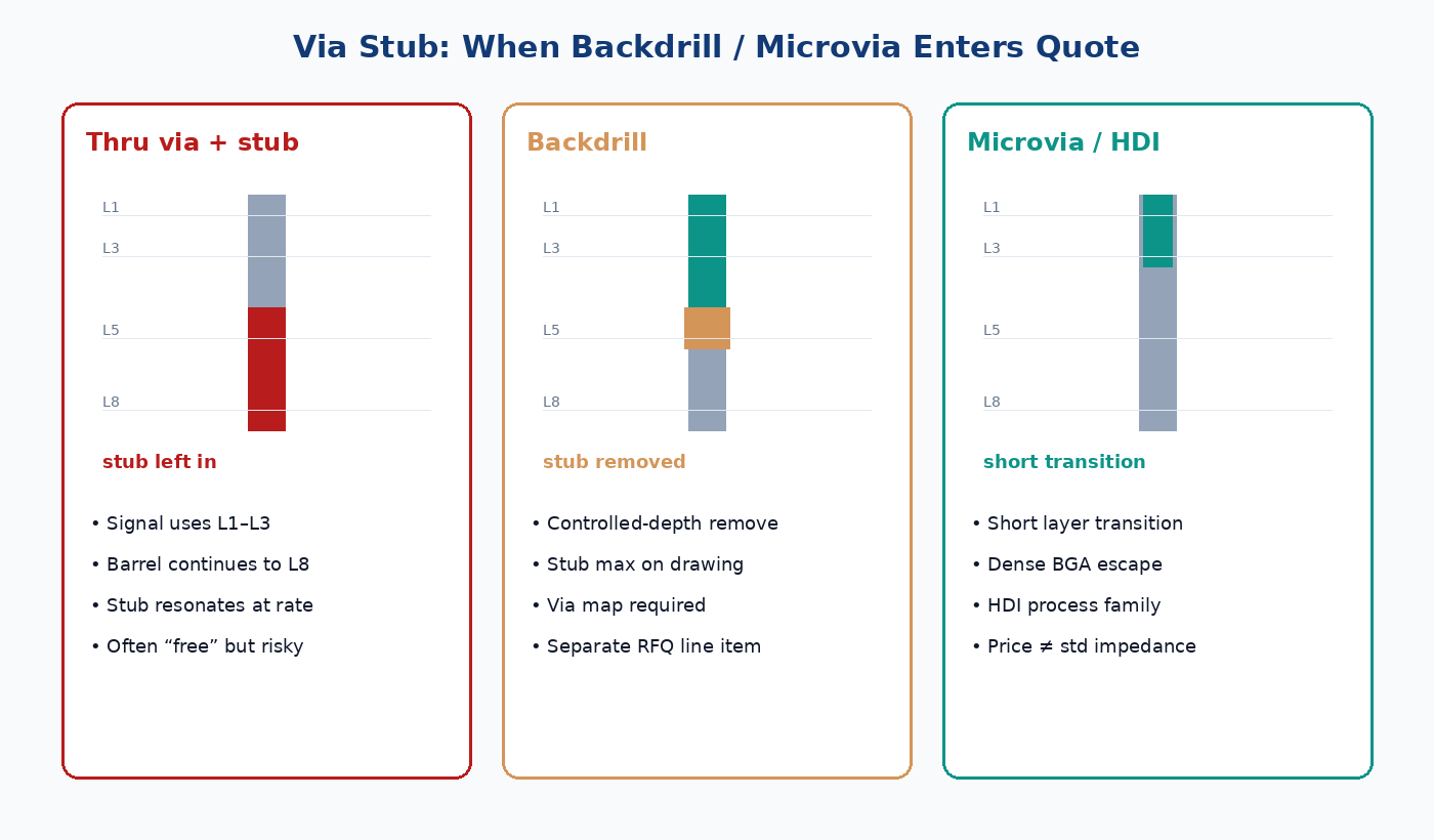
A through-via that only needs to connect L1–L3 on a 1.6 mm 8–12 layer board still drills through the full stack. The unused barrel below the signal layer is a stub. At rising edge rates used by USB3 / PCIe / HDMI high-speed lanes, stub resonance eats margin.
| Via strategy | When it shows up in RFQ | Cost / lead-time signal |
|---|---|---|
| Matched thru vias, short stub OK | Thin boards, lower rate, short stubs | Usually in base controlled-impedance price |
| Backdrill (controlled depth) | Thick boards, multi-Gbps, long stubs | Separate line item; need drill map + stub max |
| Blind / buried / microvia (HDI) | Dense BGA escape + short transitions | HDI process family; not “free with impedance” |
| Via-in-pair symmetry | Always for diff | Same layer transition, same stub treatment on both legs |
Symmetry rule: if P goes through a via, N needs the same via type, layer change, and stub treatment. One-sided backdrill or a plane clearance under only one pad is a common China DFM fail that still “passes” netlist length match.
Ask for: backdrill yes/no, max stub length (mils), which nets/vias, and whether microvia is allowed as an alternative. Silent RFQs get silent stubs.
China fab RFQ matrix for differential pairs
Paste this into the quote package so bidders price the same job:
| RFQ field | What to specify | Fail mode if missing |
|---|---|---|
| Zdiff list | Per structure: name, ohms, ±tol, layer, type | Generic “impedance PCB” quotes |
| Stackup lock | Customer stackup or fab proposal with written Dk lock | Mid-build dielectric swap |
| Tolerance | ±10% standard vs ±5% tight | Apples-to-oranges unit price |
| TDR coupon | Required on panel / board; report with lot | Unverifiable verbal pass |
| Backdrill | Yes/no + stub max + via map | Stub left in at rate where it hurts |
| Copper / finish | Finished oz + surface finish for outer Zdiff | Outer microstrip drift |
| Length / skew rules | Intra-pair + any inter-pair class | CAD rule ≠ fab check |
| Material class | FR-4 / mid-loss / low-loss; weave note if needed | Wrong laminate family |
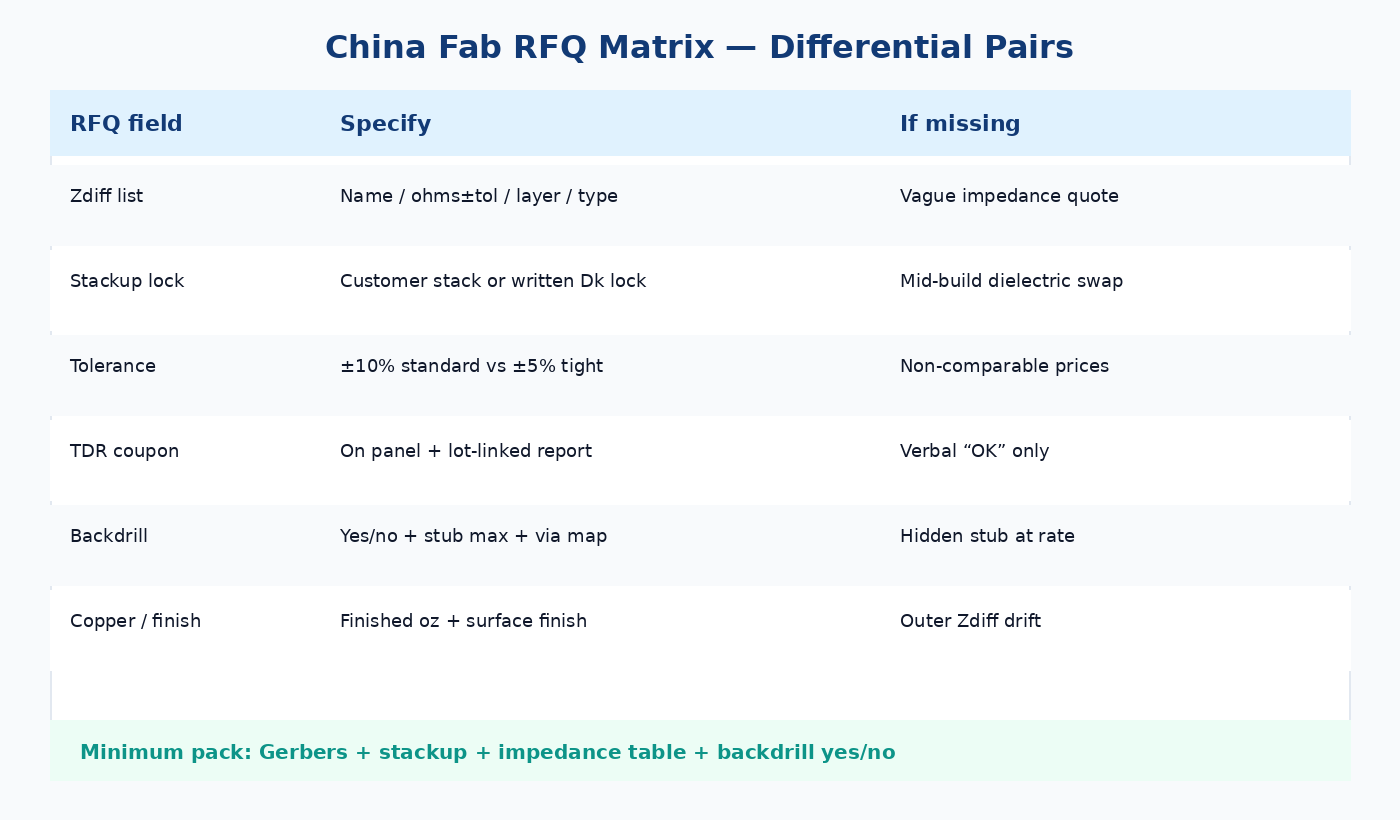
Minimum viable controlled-impedance RFQ: Gerbers + stackup table + impedance table (structure/ohms±tol/layer/coupon) + backdrill yes/no. Everything else is how you keep the second and third bidder honest.
Split-plane and reference traps buyers still miss
Zdiff calculators assume a continuous reference under the pair. On real China fab panels, the common failures are:
| Trap | What happens | Drawing / RFQ fix |
|---|---|---|
| Plane split under one leg | Return path discontinuity → mode conversion | Forbid splits under DP_* structures; stitch GND with via fence if a gap is unavoidable |
| Void for connector anti-pad | Local Zdiff bump and skew near the launch | Show keep-out; length-match after the void region in SI notes |
| Layer hop without ground via | Return current loops far from the pair | Require adjacent GND vias at every diff via transition |
| Mixed ref (GND then power) | Unexpected Zdiff and crosstalk | Name the reference net per structure in the impedance table |
If the layout tool reports “length matched” but one net crosses a split and the other does not, the fab will still etch what you drew — and the PHY will still fail SI. Put the continuous-reference rule on the fab notes so CAM raises a DFM flag instead of silently processing.
Soft close for XFPCB buyers
If you already have a stackup and Zdiff table, send them with the Gerber set and ask for a locked stackup + TDR coupon quote — not a brochure claim of “impedance capable.” XFPCB can review differential-pair structures, propose etch/finish assumptions in writing, and flag when backdrill or HDI is the cheaper way to kill stubs versus hoping FR-4 and luck will hold the eye.
Bring the Zdiff list, stackup lock, ±10% vs ±5% choice, coupon requirement, and backdrill map in the first email. That package is what turns “China PCB impedance quote” into a comparable factory bid instead of a marketing checkbox.
Start from the impedance and dielectric primers linked above, then attach the RFQ matrix on this page so every China fab answers the same questions.