
Place first, route second, release only when the package is fab-ready. PCB board design that survives first assembly follows a fixed workflow: freeze footprints and netlist, place in a manufacturable order (connectors to protection to critical ICs to power to decoupling to the rest), keep return paths continuous under fast edges, then ship Gerbers with notes a CAM engineer can build without guessing. This guide is the full layout workflow for overseas EE and procurement -- placement habits, zoning, return copper, thermal relief vs tombstone, fiducials, DFA spacing, and the pre-order checklist you should demand from the design house. It is not a package-material EMI essay, not a stackup encyclopedia, and not a regulator hot-loop deep dive; those live in separate XFPCB guides.

Layout is three stages -- schematic freeze, place/route, release package
Treat layout as three gates with exit criteria, not an open-ended drawing session that ends when the last net turns green.
| Stage | Exit criteria | Typical failure if skipped |
|---|---|---|
| Schematic / library freeze | Footprints match datasheets; netlist and BOM rev locked; pin swaps documented | Pad-to-pin mismatch, wrong package, late ECO after Gerber |
| Layout (place then route) | Mechanical keep-outs honored; zones placed; return copper continuous under fast nets; DRC + DFA clearances | Tombstone, EMI from split returns, connector interference |
| Release package | Gerber/ODB++, drill, stackup, fab notes, pick-place, BOM, fiducials -- revision-aligned | CAM hold, quote churn, wrong finish or outline |
Procurement should refuse to open price comparison until stage-three artifacts exist at one revision. A pretty board screenshot is not a release package.
Footprint and netlist pitfalls that burn the first spin
Most first-article scrap starts before a single trace is routed: wrong lands, wrong pin maps, and BOM lines that do not match the library.
- Footprint pad size and pitch copied from a similar part instead of the exact datasheet land pattern.
- Through-hole connector footprint missing mechanical keep-out or mounting holes called on the housing drawing.
- Pin-1 silk vs pin-1 copper disagreement after a library mirror or rotation.
- Netlist exported from a schematic rev that no longer matches the BOM line items.
- Thermal-pad vias omitted on QFN/QFP exposed pads, or vias left open so paste wicks into barrels.
- Courtyard and 3D body height ignored against enclosure or daughtercard clearance.
Watch Out for: Releasing Gerbers while the BOM still lists "TBD" alternates for fine-pitch ICs. Assembly builds the pick-place file against the BOM; CAM builds copper against Gerber. Divergent revs are how you buy two wrong boards.
Freeze the library, run a BOM-to-schematic-to-netlist cross-check, then open the layout editor. Place-then-route is a sequence, not a slogan.
Placement sequence that protects yield
Place in this order every time: connectors and mechanicals first, then protection, then critical ICs, then power stages, then decoupling, then everything else -- each step tagged for the yield risk it controls.
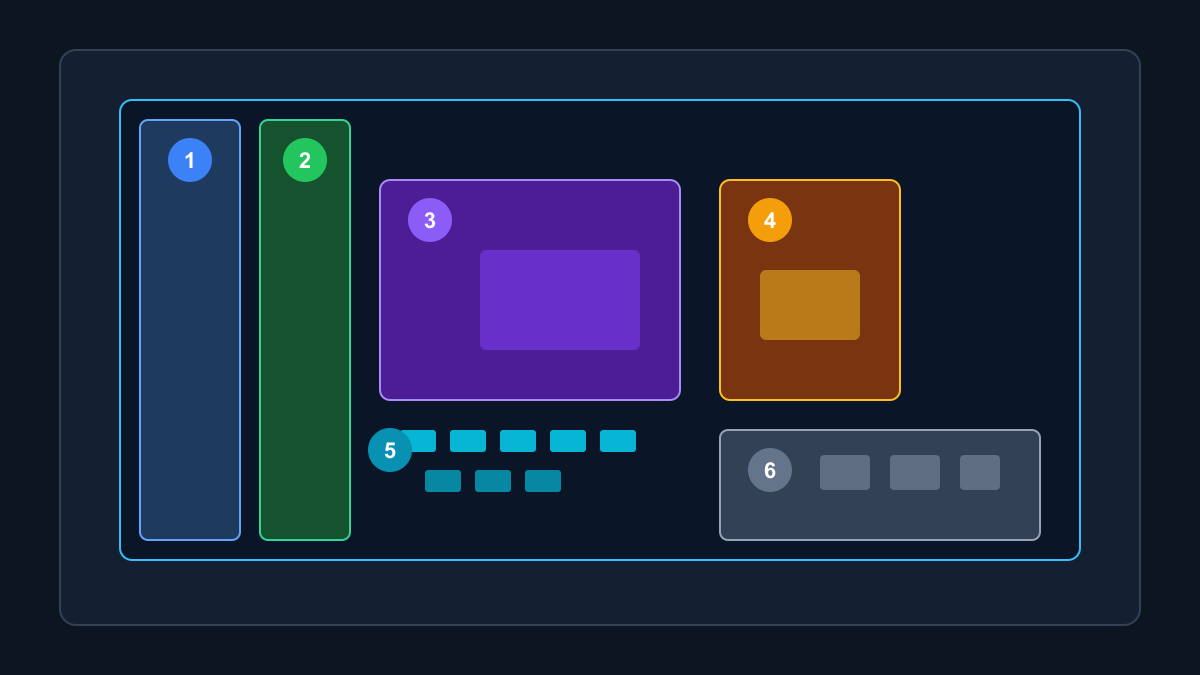
- Connectors and board-edge mechanicals -- yield tag: fit / mating. Lock mating faces, board outline, mounting holes, and keep-outs against the enclosure. Routing around a connector you moved later is wasted work.
- Input protection and interface clamps -- yield tag: surge path. Put TVS, common-mode chokes, and filter networks next to the connector they protect so the unprotected stub stays short.
- Critical ICs (MCU, FPGA, RF, high-speed SERDES) -- yield tag: SI / escape. Park the hard packages where escape routing, crystal/clock keep-outs, and continuous reference copper are still available.
- Power stages and regulators -- yield tag: thermal / hot-loop. Place switchers and LDOs with short hot loops and copper for heat before glue logic fills the neighborhood.
- Decoupling and local bypass -- yield tag: PDN / reflow. Drop ceramics next to power pins with short vias into planes; balance pad copper to limit tombstone on 0402/0201.
- Remaining glue logic, indicators, test points -- yield tag: DFA access. Fill last so AOI, probe, and rework access stay open around the dense zones.
Functional zoning is the map under that sequence: keep noisy switchers and clocks physically away from quiet analog/RF; keep digital return domains intentional; do not sprinkle LEDs and test pads inside fine-pitch BGA parks. Zoning is placement language CAM and assembly both understand.

Agree the stackup early enough that placement knows which layer is the unbroken reference under high-speed corridors. A stackup decided after routing usually means return-path surgery.
Grounding and return paths: unbroken copper under fast edges
Fast edges return on the nearest continuous reference under the trace; a split, slot, or unstitched gap forces a long detour that radiates and couples -- keep that return copper unbroken under clocks, differential pairs, and reset/IRQ edges.
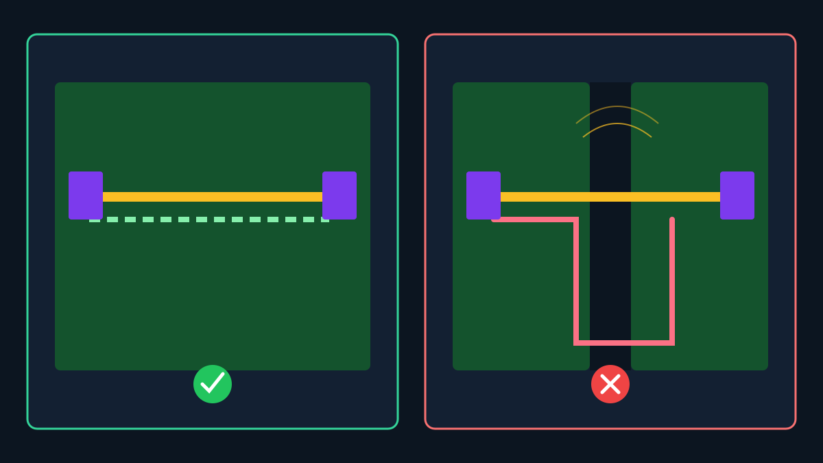
Practical layout habits:
- Route high-speed and sensitive nets over solid GND (or a deliberate reference plane) with no plane splits under the route.
- If power and ground must change domains, stitch with vias near the crossing or move the crossing to a quiet region -- do not leave a lone signal over a slot.
- Prefer short return vias next to signal layer changes so the loop stays small.
- On two-layer boards, dedicate as much of one side as practical to continuous ground pour with stitching; do not treat "pour everything leftover" as a reference plane.
- Separate analog and digital grounds only when the circuit needs it, then join at one intentional point -- accidental multi-point bridges defeat the split.
Return-path discipline is cheaper EMI control than adding cans after the chamber fails.
Routing and power notes that survive the fab floor
Route power and critical nets with current, inductance, and etch yield in mind -- not only DRC green.
- Size power traces and plane necks for continuous current plus margin; confirm copper weight on the stackup note matches the ampacity assumption.
- Keep switch-node and hot-loop areas compact; long skinny necks under a FET or inductor raise both loss and EMI.
- Prefer 45-degree or curved transitions over acute corners on etch-sensitive fine lines; leave clearance above the fab's published minimum, not at the absolute process floor.
- Length-match only where the interface guide requires it; decorative matching that crosses splits is worse than a short unmatched run over solid reference.
- Via-in-pad on fine pitch needs filled/capped callouts in fab notes, or solder wicks into open barrels.
Thermal relief vs tombstone on small passives: thermal relief spokes on large pours help hand and wave soldering, but unequal copper on the two pads of an 0402/0201 is a classic tombstone driver in reflow. Match pad copper and spoke count on small chip parts; do not hang one terminal on a solid pour and the other on a skinny neck. For dense SMT, follow DFA spacing so nozzles, AOI cameras, and rework tips can reach neighbors -- courtyard-to-courtyard clearance is an assembly rule, not decoration.
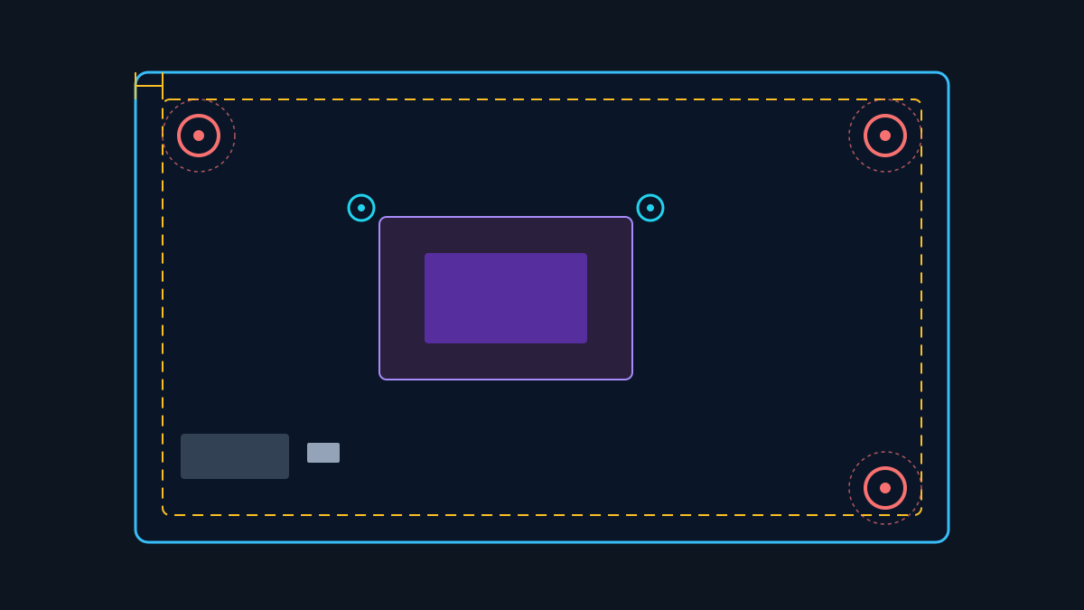
Fiducials: put three global fiducials in an L-pattern near the board corners for panel and board alignment, with copper-free keep-out around each mark per the assembler's recipe. Add local fiducials beside fine-pitch BGA/QFN when the pick-and-place program needs them. Keep components and copper pours out of the outline clearance the fab and depaneling process require.
Release package and DFM checklist before you order
Ship a revision-locked release package; Gerbers alone without stackup, drill, and fab notes are an invitation for CAM to invent your board.
What belongs in fab notes (minimum):
- Board outline, thickness, layer count, and copper weights per layer
- Material / Tg (and impedance targets with reference layers if controlled impedance)
- Surface finish name and thickness window where relevant
- Solder mask and silkscreen color; mask expansion / min dam if non-default
- Drill table: plated vs non-plated, tolerances, any back-drill or filled via callouts
- Impedance coupon presence; panelization preferences if you care
- Special: edge plating, gold fingers, scoring/V-cut, keep-outs, UL marks
Pre-order checklist procurement can demand from the design house
PCB layout release checklist (design house -> buyer -> fab)
- [ ] Schematic, BOM, and netlist at one locked revision
- [ ] Footprint audit vs datasheet for connectors + fine-pitch ICs
- [ ] Placement order / zoning review signed (connectors -> protection -> critical -> power -> decap -> rest)
- [ ] Return-path review: no splits under clocks / differential / reset
- [ ] Stackup table attached (layers, copper oz, dielectric, Tg)
- [ ] DFA spacing reviewed for SMT nozzles / AOI / rework
- [ ] Global (3) + local fiducials placed with keep-outs
- [ ] Thermal relief balanced on 0402/0201 and smaller
- [ ] Gerber or ODB++ + NC drill + pick-place (CPL) + fab drawing
- [ ] Fab notes: finish, mask, impedance, via-fill, outline tolerances
- [ ] DRC + assembly DFM report attached (not only "DRC clean")
- [ ] Change control: no silent footprint or stackup swap after PO
Procurement Pro-Tip: Put the checklist above in the RFQ as buyer acceptance criteria. Quotes that arrive without stackup, finish callout, and fiducial confirmation are not comparable -- they are bids on different imaginary boards.
Watch Out for: "Panel ready" claims with only two fiducials, no local marks next to 0.4 mm pitch BGA, and outline copper inside the depaneling keep-out. That package will bounce at CAM or at the SMT line.
Related XFPCB guides
- PCB DFM: Design for Manufacturing -- CAM questions that still appear after DRC passes
- PCB Design Guidelines That Prevent Rework -- packages, materials, EMI zoning, and copper heat paths
- Multilayer PCB Stackup Fabrication Guide -- layer order, reference planes, and fab-ready stackup tables
- PMU PCB Design Guide -- power-stage layout, hot loops, and thermal vias for regulator islands