
PCB assembly equipment is the set of machines that deposit solder paste, place parts, reflow or wave solder, inspect joints, and electrically test a finished PCBA. For overseas buyers sourcing China PCBA, the useful question is not "do you have SMT?" — almost every brochure says yes — but which stages are in-house, which packages those machines actually run at yield, and which inspection/test steps are required for your BOM versus optional for simple boards.
This page maps the line by stage, flags when SPI / 3D AOI / X-ray stop being nice-to-have, compares ICT vs flying probe vs functional test by volume and NRE, corrects the lead-free (SAC) reality after years of SnPb-default marketing copy, and closes with an RFQ matrix you can paste into a China PCBA quote request.
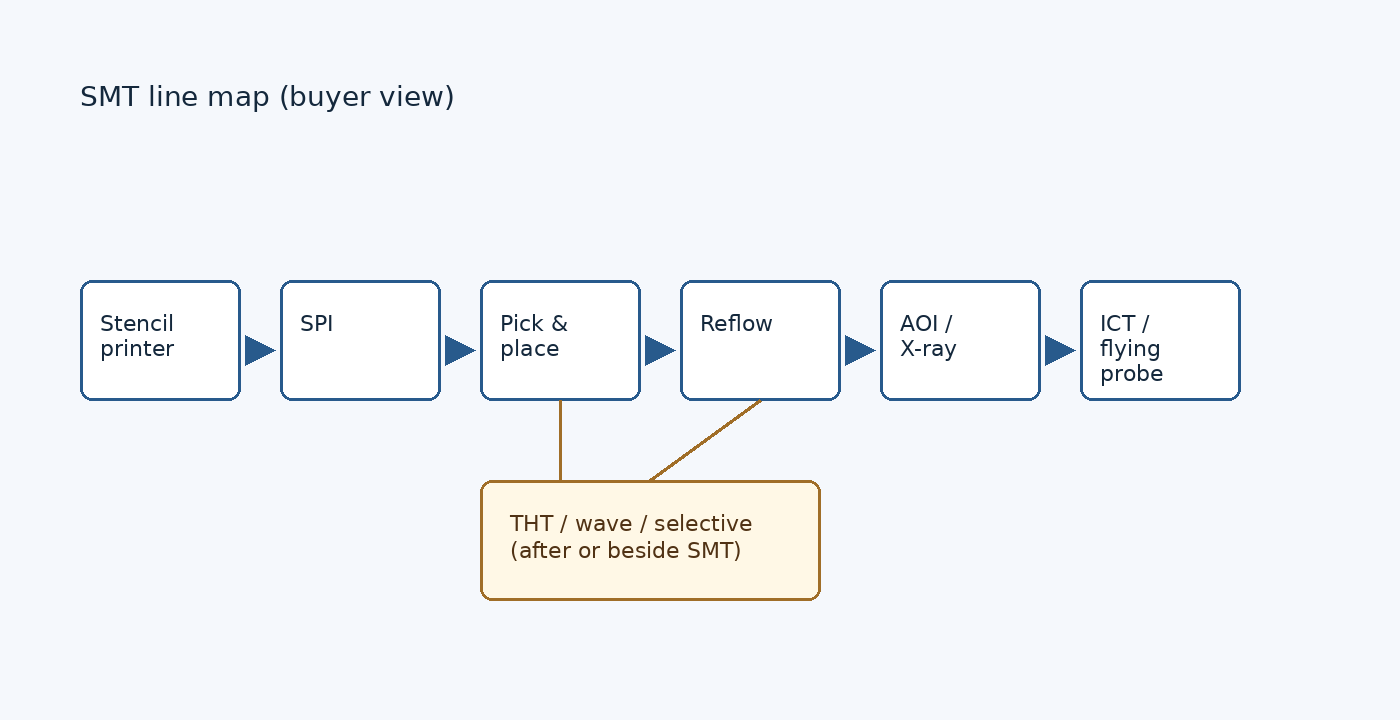
SMT stage map (and where THT fits)
Most turnkey China PCBA lines are SMT-first. Through-hole (THT) still matters for connectors, power parts, and transformers — it sits beside or after SMT, not as a separate "museum" process.
| Stage | Equipment | What it actually does | Buyer signal to ask |
|---|---|---|---|
| Paste | Stencil printer (auto/semi) | Presses solder paste through a metal stencil onto pads | Stencil type (laser/step), support pins, under-stencil clean |
| Paste check | SPI (solder paste inspection) | Measures paste volume/height/area before parts land | % of boards with SPI; reject limits; 2D vs 3D |
| Place | Pick-and-place (chip shooter + multi-function) | Picks reels/trays and places SMDs to coordinates | Min pitch, 0201/01005, BGA/CSP capability, feeder count |
| Reflow | Reflow oven (air or nitrogen) | Melts paste into solder joints on a thermal profile | Zone count, N2 availability, profile coupon on FA |
| Optical | AOI (2D/3D) | Looks for missing/skewed parts, solder defects | 3D vs 2D; coverage rule (100% vs sample) |
| Hidden joints | X-ray (2D/3D/CT as needed) | Sees BGA/QFN voids and bridges under packages | When X-ray is mandatory on your PO |
| THT | Wave and/or selective solder | Solders through-hole leads after SMT (typical order) | Mixed-tech sequence; selective for dense SMT near THT |
| Electrical | ICT, flying probe, functional | Opens/shorts, component values, or system behavior | Fixture ownership; coverage; NRE vs unit cost |
Wave solder is still common for connector-heavy boards. Selective solder is what you want when tall SMT parts sit next to THT pins and a full wave would heat-damage or bridge. Hand solder remains for odd parts and ECO rework — do not treat it as a substitute for a documented selective process when volume rises.
💡 Procurement Pro-Tip: Ask for the traveler sequence in writing: SMT bottom → reflow → SMT top → reflow → THT → selective/wave → wash (if any) → coat (if any) → pack. Mixed-tech boards fail quotes when the plant assumes a sequence you never approved.
Stencil printer and SPI
The printer sets paste volume. Too little paste → opens on fine pitch; too much → bridges and solder balls. Auto printers with vision alignment beat manual benches on fine pitch, but the machine brand on the wall matters less than stencil design (aperture reduction, step-down for large pads next to fine pitch) and cleaning frequency.
SPI sits after print. It is the earliest hard gate on the line: bad paste never becomes a "mystery" after reflow.
When buyers must require SPI
- 0.5 mm pitch and finer, micro-BGAs, fine QFNs
- High reliability (automotive, medical, industrial controls)
- First-article and early production on a new stencil
- Any board where paste volume is already a known yield driver
When SPI can stay optional / sample
- Coarse pitch, mostly 0603+, few ICs, no bottom-terminated packages
- Stable high-volume job with a proven stencil and low DPI history (still sample SPI periodically)
⚠️ Watch Out for: A plant that "has SPI" but only runs it for customer audits. Put SPI coverage % and reject criteria in the PO, not in a hallway promise.
Pick-and-place
Chip shooters place small passives fast; multi-function heads place ICs, connectors, and odd-forms. Capability claims to check:
- Minimum passive size (0201 / 01005)
- Minimum IC pitch and BGA ball pitch
- Package types: QFN, LGA, POP, tall connectors
- Dual-lane vs single-lane (throughput, not quality by itself)
- Traceability: feeder/setup verification, moisture-sensitive device (MSD) control
Prototype vs volume: the same brand of placer can run both, but feeder setup, program optimization, and nozzle libraries differ. A line that is efficient at 5k/month may still stumble on a 20-piece NPI with twenty unique odd-forms if engineering time is not quoted.
Reflow oven — and lead-free SAC reality
Reflow turns paste into joints. Zone count, conveyor stability, and nitrogen option matter more than the logo on the oven sheet.
Many older marketing tours still talk as if SnPb paste were the default. For most commercial electronics sold into the EU, China export, and global OEM channels, lead-free SAC alloys (e.g. SAC305-class) are the default. SnPb remains for exempt products and some repair/legacy lines — it is not what you should assume on a China PCBA quote unless you explicitly specify an exemption and alloy.
Lead-free profiles run hotter. That raises the value of:
- Nitrogen (reduces oxidation, can improve wetting on tough finishes)
- A documented profile on a coupon or sacrificial board for first article
- Correct PCB finish and component temp ratings matched to the profile
💡 Procurement Pro-Tip: On the RFQ, write the alloy (SAC305 or your AVL), whether N2 is required, and that first-article must include a profile graph. "RoHS line" alone does not lock those three.
AOI and X-ray
AOI catches visible defects: missing parts, polarity, tombstones, many solder bridges. 3D AOI adds height/volume context that 2D misses on some solder joints.
X-ray is for joints you cannot see: BGA balls, many QFN/LGA pads, some connector underfills shadows.
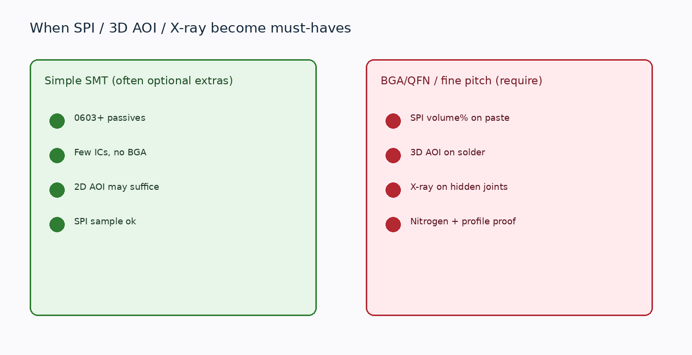
Require 3D AOI / X-ray when
- Any BGA, CSP, or bottom-terminated package where opens hide under the part
- Fine-pitch connectors with hidden solder
- Automotive / medical / high-reliability acceptance that already names X-ray sampling plans
Optional for simple boards
- Low-density SMT with gull-wing SOIC/QFP and chip passives only — 2D AOI + visual may be enough if yield history is proven
Do not confuse "we own an X-ray" with "every board is X-rayed." Coverage belongs in the quality plan: 100%, first-article only, or AQL sample.
ICT vs flying probe vs functional test
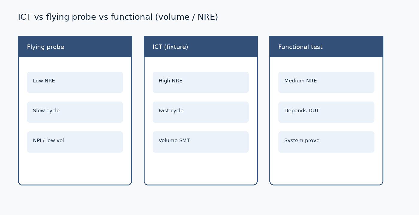
| Method | NRE | Cycle time | Best fit | Weak spot |
|---|---|---|---|---|
| Flying probe | Low | Slow | NPI, low volume, frequent ECO | Throughput; limited power-up |
| ICT (bed-of-nails) | High (fixture) | Fast | Stable volume, dense nets | Fixture cost/ownership; design-for-test pads |
| Functional / FCT | Medium | Varies | System-level prove-out | Debug depth; fixture + software effort |
Rule of thumb: flying probe for prototypes and low volume; ICT when monthly volume amortizes the fixture; functional test when the customer cares about I/O behavior, firmware load, or calibrated outputs that ICT cannot see.
Ask who owns the ICT fixture after NRE: customer-owned tooling that can move with the job vs plant-owned tooling that locks you in. Put ownership and storage in the contract.
Prototype vs volume — same machines, different gates
| Topic | Prototype / NPI | Volume |
|---|---|---|
| Printer | Manual/semi acceptable for coarse pitch; auto preferred for fine pitch | Auto printer + SPI discipline |
| SPI | Strongly recommended on fine pitch NPI | Locked coverage % |
| Placer | Flexibility > pure speed | Optimized feeders, dual-lane if quoted |
| Reflow | Profile work is part of NPI cost | Golden profile + periodic verification |
| AOI/X-ray | First-article heavy | Sample plan tied to DPPM goals |
| Test | Flying probe / limited FCT | ICT + FCT as designed |
A China PCBA partner that only shows a photo of a high-speed placer has not answered NPI engineering time, stencil revisions, or how ECO stops are handled mid-lot.
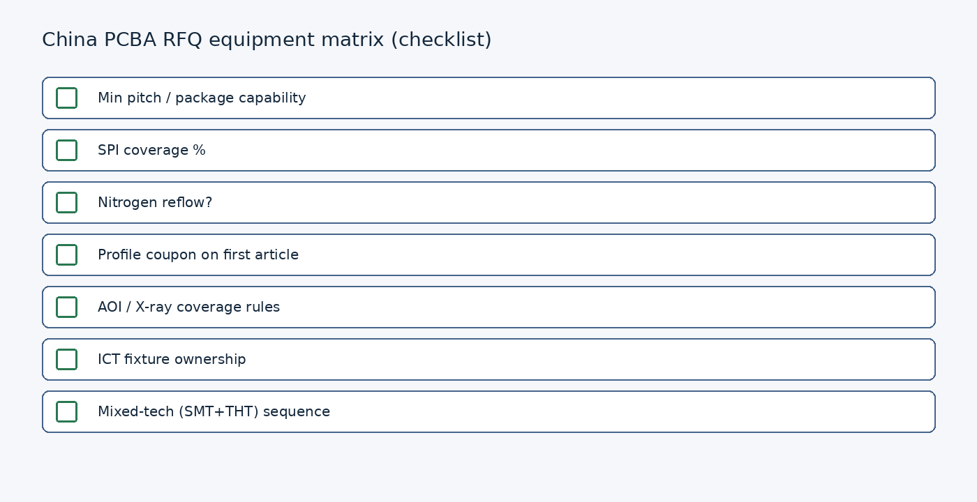
China PCBA RFQ equipment matrix
Use this table as a paste-ready checklist. Brochure lines fail here; capable partners answer in specifics.
| RFQ field | Why it matters | Example answer format |
|---|---|---|
| Package / pitch capability | Separates real fine-pitch lines from marketing | "01005; 0.4 mm BGA; QFN wettable flank OK" |
| SPI coverage | Paste defects caught early | "100% SPI on all lots; reject at ±xx% volume" |
| Nitrogen reflow | Wetting / cosmetics on lead-free | "N2 available; used when PO requires" |
| Profile coupon | Proof the oven matches your stackup | "FA includes profile graph on coupon" |
| AOI / X-ray coverage | Hidden joint risk | "100% 3D AOI; X-ray 100% on BGA / sample on QFN" |
| ICT fixture ownership | Exit cost if you move plants | "Customer-owned; stored tagged at CM" |
| Mixed-tech sequence | SMT+THT yield | "SMT both sides → selective THT → wash → coat" |
| Alloy | Stops SnPb-by-habit | "SAC305 unless exemption stated" |
Related process depth: SMT PCB assembly process, advanced PCBA equipment, full turnkey vs consignment, and PCB inspection methods.
What "capable" looks like beyond the machine photo
A capable China PCBA partner can show more than a shiny placer photo:
- Stencil process control — who designs apertures, how step stencils are approved, and how under-stencil cleaning is logged.
- Moisture and MSD handling — dry cabinet policy, floor-life tracking, and bake rules when bags are open too long.
- Solder paste logistics — cold-chain, thaw time, jar life on the printer, and alloy lot traceability to the traveler.
- Changeover discipline — how feeders are verified after a BOM ECO mid-lot; barcode or scan checks beat tribal memory.
- Defect taxonomy — DPI/DPPM reviewed with paste, placement, and reflow buckets, not a single vague "SMT yield" number.
If a salesperson answers every question with a brand name and never with a coverage %, you are still shopping brochures.
Selective solder and wave — buyer traps
Wave solder is efficient for many THT pins facing the same direction with decent spacing. It becomes a trap when:
- SMT parts on the wave side cannot take wave heat
- Fine-pitch THT connectors sit in a dense SMT neighborhood
- You need different solder alloys or fluxes than the wave pot holds
Selective solder (mini-wave nozzles or dip fountain) costs more per joint but protects nearby SMT and keeps heat local. On the RFQ, require the plant to mark wave vs selective vs hand on the traveler for each THT part class — not a single checkbox "THT OK."
Hand solder is fine for true odd-forms and ECO bridges. It is a red flag when the quote uses hand solder as the plan for hundreds of dense THT pins on a production release.
Soft next step
If you already have Gerbers, BOM, and centroid data, XFPCB can map this equipment checklist onto your package list and reply with which gates (SPI, N2, X-ray, ICT vs flying probe) belong in the quote — without forcing a fixture you do not need on a 50-piece run.
⚠️ Watch Out for: Quotes that only list machine brands. Brands do not ship your boards — coverage rules, alloy, profile proof, and fixture ownership do.