
The board left AOI with a clean traveler. Pads looked wet, polarity marks matched the program, and every visible package sat inside its placement window. Six weeks later a field unit dropped a sensor under vibration. Bench continuity still passed at room temperature. X-ray on the returned board showed corner balls under a fine-pitch BGA joined by a narrow waist -- head-in-pillow that cameras never saw. A second return from the same lot had a resistor that photographed correctly and measured the wrong value. That is the procurement problem this guide solves: inspection clauses that name the methods that catch what looks fine, and the methods that still miss function.
This article is for quality and sourcing engineers writing RFQ inspection language for China PCBA. It separates inspection from test, maps defect families to the earliest cheap gate, walks the line from MVI through SPI, AOI, selective X-ray, flying probe or ICT, and FCT, then shows how fabs typically tier coverage for prototype, volume, and Class 2 / Class 3 risk. It is a process inspection stack -- not a field remake decision guide and not a schematic bring-up plan.
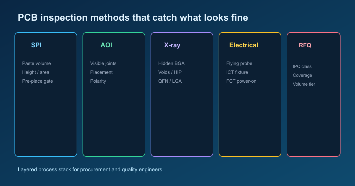
Inspection versus test: two questions, two tool sets
Inspection asks whether paste, parts, and joints are physically correct. Cameras, operators, and X-ray read shape, registration, and density. Test asks whether the assembled circuit behaves electrically and functionally. Probes and powered jigs read resistance, values, polarity, net integrity, and product behavior under load.
A part can pass optical inspection and still be the wrong value or internally open. A functional test can pass while a marginal hidden joint quietly degrades under heat and vibration. Optical coverage and electrical coverage are complementary layers. RFQ language that names only AOI, or only FCT, leaves a blind spot the other family owns.
Bare-board electrical continuity before assembly is a third gate. It confirms copper nets on the fabricated board. Assembled ICT or flying probe confirms components and joints after SMT. Neither replaces the other, and neither replaces powered functional test when firmware and interfaces matter.
Defect families: paste, placement, solder, board
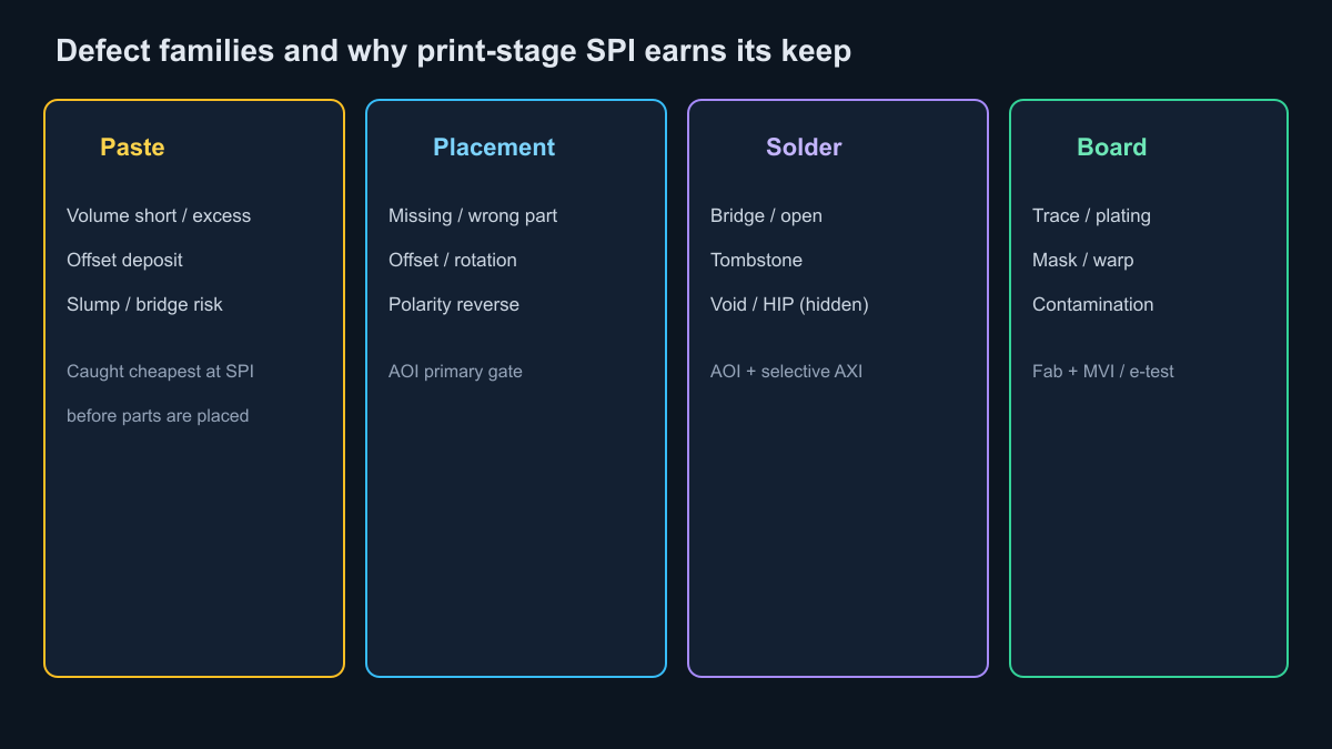
Most assembly escapes fall into four families:
- Paste: short or excess volume, offset deposits, slump that becomes a bridge after reflow.
- Placement: missing parts, wrong parts, offset or rotation, reversed polarity.
- Solder: bridges, opens, insufficient fillets, tombstones, voids, head-in-pillow under bottom-terminated packages.
- Board: damaged traces, plating issues, mask defects, warpage, contamination that survived fab gates.
Industry process data commonly attributes a large share of SMT solder problems to the stencil print step -- often cited in the 30% to 60%+ range depending on study and product mix. The exact percentage matters less than the cost curve: a print miss fixed at SPI is a reprint; the same miss after reflow is scrap, rework, or a field return. That is when SPI earns its keep -- fine pitch, bottom-terminated packages, Class 2 / Class 3 risk, or any line where paste volume drives yield.
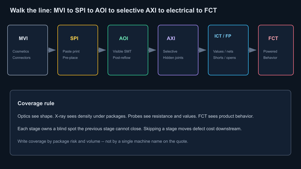
Walk the line: MVI to SPI to AOI to selective AXI
Manual visual inspection (MVI)
A trained operator with magnification still owns cosmetics, connector seating, labels, hardware, and coating coverage that automation misjudges. Effectiveness falls as pitch shrinks and density rises. Fatigue and line-of-sight limits make MVI a support gate, not the sole gate for fine-pitch SMT.
Solder paste inspection (SPI)
SPI runs after stencil printing and before placement. 3D systems measure height, area, volume, and alignment on each pad. A starved aperture, clogged stencil, or misregistered print is corrected before parts are placed. Require SPI when the BOM includes fine pitch, BGA / QFN / LGA, or when first-article paste windows are unstable. For simple low-density prototypes without hidden joints, some programs defer SPI and accept higher print risk -- write that choice explicitly so quotes stay comparable.
Automated optical inspection (AOI)
AOI compares the board to CAD or a known-good reference under controlled lighting. It catches missing and misaligned parts, polarity errors, tombstones, bridges, and many visible fillet issues. Pre-reflow AOI can stop placement errors before solder forms; post-reflow AOI judges finished joints on exposed leads and chips. Hard limit: joints under package bodies are outside the camera view. AOI confirms the outer edge of a BGA is present and seated; it does not inspect the balls underneath.
Selective automated X-ray (AXI)
X-ray reads density. Solder absorbs more than plastic and FR-4, so hidden balls and pads appear for void, open, bridge, and head-in-pillow review. 2D transmission is fast for gross defects; oblique or 3D modes separate overlapping features and support void measurement. Equipment time and operator skill make AXI selective: apply it to BGA, QFN, LGA, and other high-risk sites, or to 100% of hidden joints when Class 3 or field history demands it. IPC-7095 guidance commonly treats projected void area above about 25% of ball area as defective; many high-reliability programs write tighter internal limits. Location at the pad interface often matters more than a raw percentage in the image center.
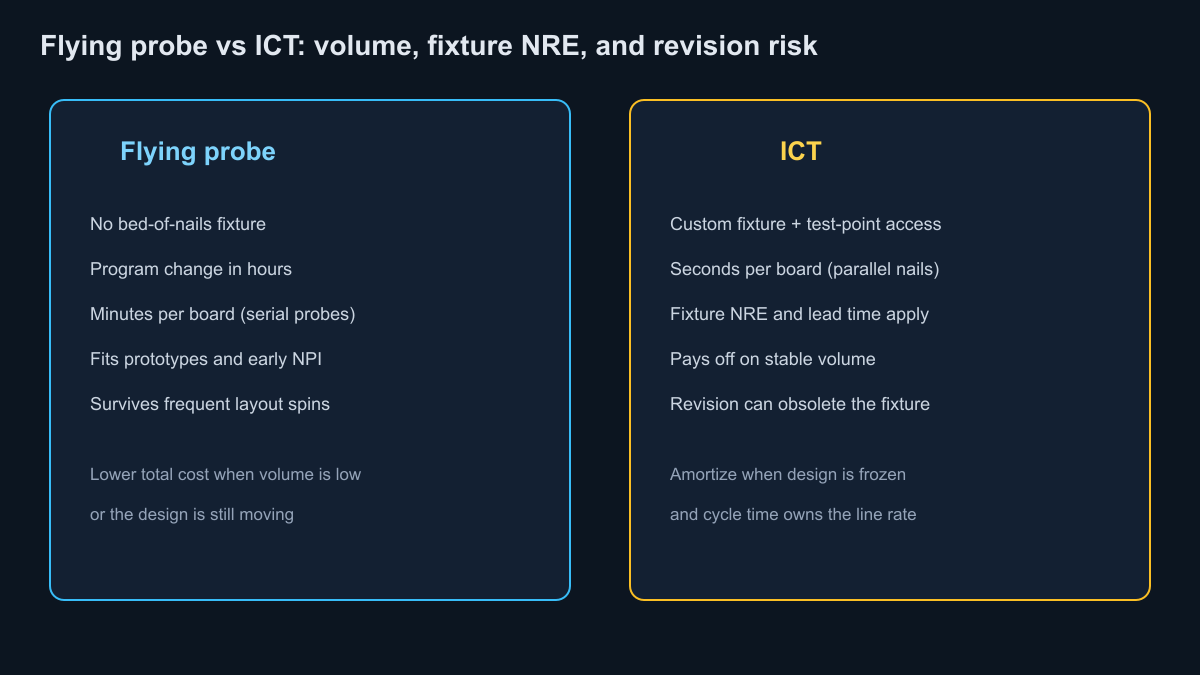
Electrical layer: flying probe versus ICT, then FCT
Wrong-value parts, high-resistance joints, and polarity errors can look acceptable in an optical image. Electrical test closes that gap.
Flying probe uses motorized probes and no bed-of-nails fixture. Programs change with a new revision. Cycle time is measured in minutes per board because probes move serially. It fits prototypes, NPI, and low-to-mid volume while the layout still spins.
ICT uses a custom fixture that contacts many nodes at once. Cycle time is typically seconds per board. Fixture NRE and build lead time apply, and a layout change can obsolete the fixture. Once volume is stable and test-point access exists, ICT amortizes against flying-probe cycle time. Break-even is a volume and revision calculation, not a slogan -- runs still changing often stay on flying probe even when unit counts rise.
Both methods check shorts, opens, many component values, and polarity when access allows. Neither proves firmware boot, interface timing, or loaded regulation. Functional test (FCT) powers the board under near-product conditions and compares outputs to pass / fail limits. FCT catches system faults that structural methods miss, and it rarely isolates which of hundreds of parts failed -- keep ICT or flying probe upstream when diagnosis speed matters. Boundary scan can extend digital coverage under packages when physical probes cannot land.
How China fabs typically tier inspection plans
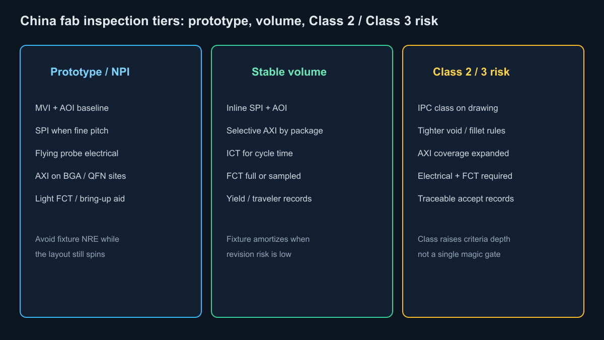
Quotes often look identical until coverage is written. Typical tiering:
Prototype and engineering validation: AOI plus flying probe, SPI when fine pitch or paste risk is real, selective AXI on hidden packages, light FCT or engineering bring-up support. Skip fixture NRE while the design moves.
Low-volume high-mix: AOI plus flying probe, SPI on fine-pitch travelers, AXI targeted to bottom-terminated parts, simplified FCT when the product warrants it. Fixture investment stays off the traveler.
Stable volume: inline SPI and AOI, selective or expanded AXI for BGA / QFN populations, ICT once the design freezes and pads exist, FCT full or sampled by risk. Yield and batch records travel with the lot.
Class 2 versus Class 3 risk: class is an acceptance depth on the drawing, not a machine name. Moving up tightens fillet, overhang, void, and cleanliness allowances and usually expands AXI and electrical / FCT coverage. State IPC-A-610 class (and soldering process expectations such as J-STD-001 where required) so CAM and QA price the same bar.
RFQ checklist language buyers can paste
Put the following on the RFQ and assembly drawing so China PCBA quotes are comparable:
- IPC acceptance class and revision for assembly workmanship (IPC-A-610); add soldering process standard if your program requires it.
- SPI: required or waived, and for which pitches / package types.
- AOI: pre-reflow, post-reflow, or both; polarity and part-mark expectations.
- AXI: list packages or sites requiring X-ray (BGA / QFN / LGA / others); 2D versus 3D if you care; void accept criteria or reference to IPC-7095 / internal limit.
- Electrical: flying probe or ICT; if ICT, confirm test-point access and who owns fixture NRE; coverage goals for shorts / opens / values.
- FCT: who supplies procedure, fixture, firmware, and pass / fail limits; sample rate versus 100%.
- Prototype versus production coverage map: what expands when volume freezes.
- Deliverables: first-article reports, AOI / AXI records, electrical / FCT logs, and batch yield notes tied to lot ID.
- One revision-aligned package: Gerbers or ODB++, centroids, BOM with MPNs, assembly drawing, and fab notes.
XFPCB builds inspection as a traveler stack matched to package risk, volume, and class -- SPI where print drives yield, AOI for visible SMT, selective X-ray for hidden joints, flying probe or ICT by economics, and FCT when powered behavior is a ship gate -- so boards that look fine still get measured where optics cannot see.
A board that looks perfect can still hide a BGA void or a wrong-value part. Inspection catches physical and measurable defects; electrical and functional tests catch connectivity and behavior. SPI pulls paste risk upstream, AOI owns visible SMT, X-ray owns hidden joints, flying probe and ICT split by volume and revision risk, and FCT closes powered product behavior. Write those layers into the RFQ so China fab coverage matches the risk you actually carry.