
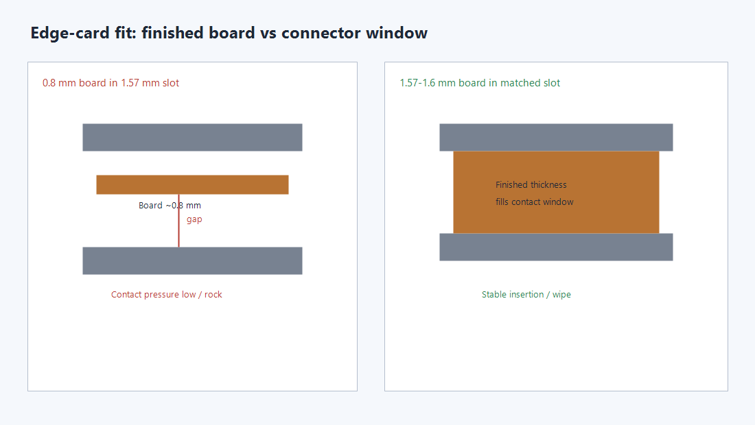
A daughtercard cut to 0.8 mm finished thickness looked fine on the layout plotters. At first article inspection it also looked fine. At the card-edge connector it failed: contacts that expect roughly 1.57 mm of board did not wipe with enough pressure, the panel rocked in the slot, and the mating cycle that worked on a 1.6 mm engineering sample became intermittent. The netlist was correct. The finished thickness was not.
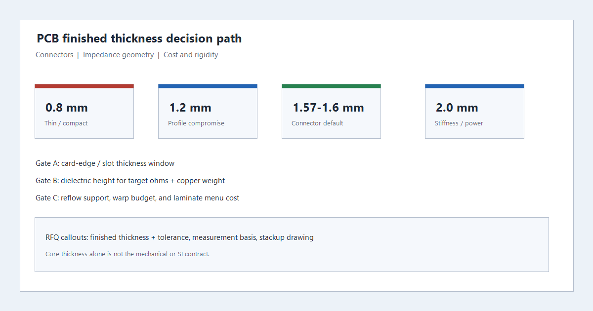
Mechanical and electrical buyers still default to 1.6 mm by habit, or jump to 0.8 mm for profile and then discover edge-card fit, reflow warp, and impedance geometry were never renegotiated. This guide follows a connector-first, impedance-second, cost-third path for choosing among common finished thicknesses from 0.8 mm through 2.0 mm -- and for writing RFQ language that CAM can build.
The 0.8 mm board that will not seat
Card-edge, board-in, and many guide-slot interfaces publish an accepted board-thickness window. That window is a finished-dimension limit, not a core-stock habit. When a design ships at 0.8 mm into hardware sized for ~1.57 mm, the usual outcomes are low contact force, rocking, intermittent wipe, and gold-finger or bevel geometries that no longer match the connector drawing.
The reverse failure is also real: a board that runs thick at the upper end of an open +/-10% band can refuse insertion or overload contacts. Before any "standard" nominal is locked, read the connector or slot drawing. If the interface is fixed, that drawing outranks catalog defaults.
Finished thickness vs the core myth
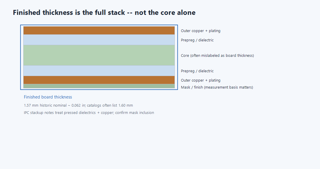
Teams often write "FR-4, 1.6 mm" and mean a core sheet. Fabrication measures a finished board: pressed dielectrics, copper foils, plating build, and -- depending on the agreed method -- coatings that sit on the surface. IPC design and rigid-board performance documents treat thickness as a construction result with a measurement basis, not as a single laminate SKU.
Two catalog numbers confuse buyers for the same historical stock:
- 1.57 mm is the de facto nominal tied to classic ~0.062 in (1/16 in class) rigid FR-4 practice.
- 1.60 mm is the common metric catalog rounding of that same family.
They are close, not identical in conversion arithmetic. Exact 1/16 in stock is 0.0625 in (~1.5875 mm). For connector work, state the finished target and tolerance you need; for quoting, confirm how the fab measures laminate-to-laminate versus any coating inclusion at critical edges.
Why 1.57-1.6 mm became the default
Presses, drill libraries, panel tooling, card guides, and edge-connector ecosystems grew up around that thickness class. Stocked cores and prepreg menus make it easy to hit near 1.6 mm on two-layer and many four-layer builds. Assembly fixtures and enclosure posts often assume the same height. That is why unconstrained boards still start there: availability and mechanical ecosystem alignment lower friction.
It remains a default, not a design rule. Layer count does not force 1.6 mm. Four-layer and higher constructions can land thinner or thicker when dielectrics and copper are chosen that way. The fab still has to prove the pressed stackup.
How thin vs thick changes impedance geometry
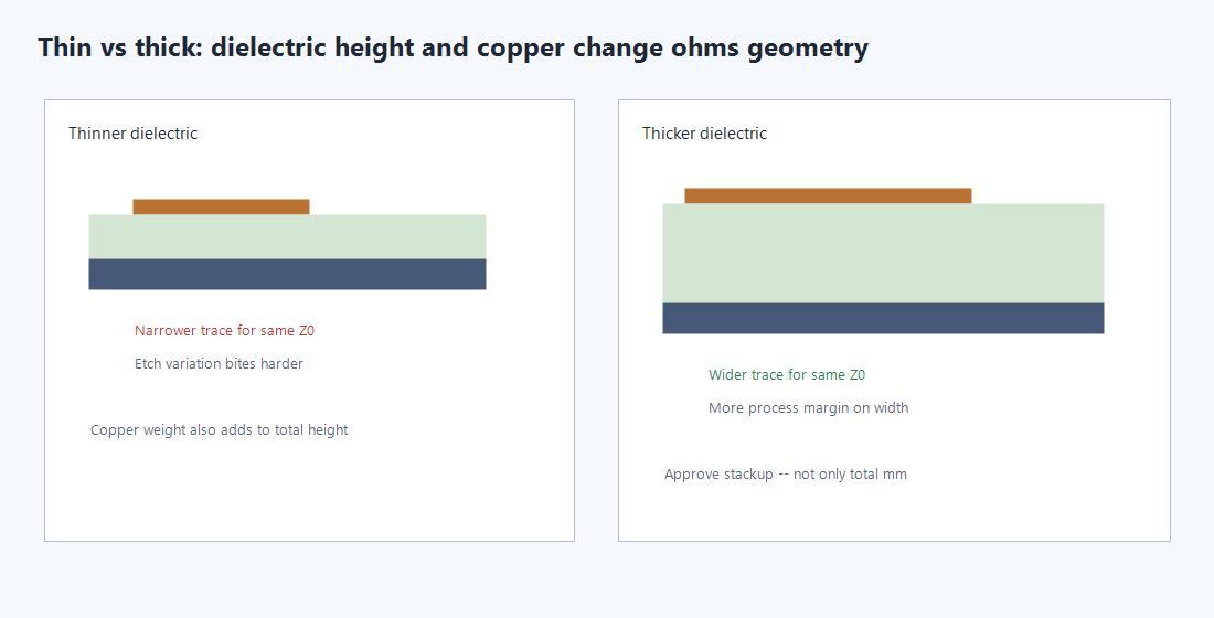
Finished thickness is not impedance by itself. Impedance follows dielectric height to the reference, copper weight, etch geometry, and resin/glass system. Changing total board height without approving the stackup redraws those variables.
On a thinner construction, dielectric height shrinks. Holding 50 ohm microstrip or 100 ohm differential usually means narrower traces. Narrower traces give etch and registration less margin, so yield and coupon scatter can worsen even when the outline looks simpler. On a thicker construction, the same ohms target often allows wider traces and more process margin -- until via aspect ratio, drill wander, and plating throw start to hurt.
Copper contributes to both ohms and total height. One-ounce foils are about 35 um; two-ounce foils are about 70 um before plating growth. Heavy copper on outer layers can move finished thickness enough to matter at a tight connector window. Specify copper weight separately from finished board thickness, and approve dielectric thicknesses on the stackup drawing rather than hoping the total millimeters alone will carry SI.
Warp, reflow support, and thin panels
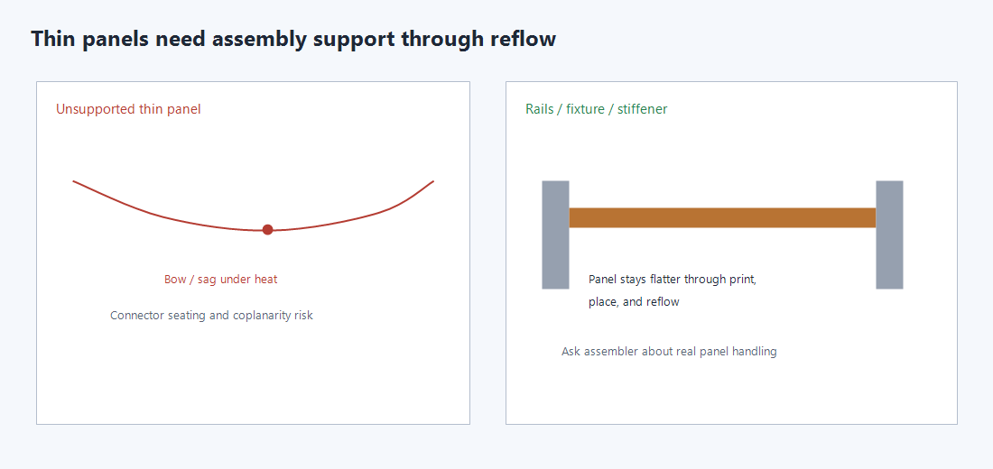
Boards near 0.8-1.0 mm flex more under print, place, and reflow heat. Bow that looks like a fixture problem often started as an unsupported thin panel or unbalanced copper. Assembly lines use rails, breakaways, carriers, and stiffeners so the real panel -- not only the singulated outline -- stays flat enough for fine-pitch parts and connectors.
Symmetry still matters: matched construction and balanced copper reduce twist after press and after thermal cycles. Thin multilayers that pack many layers into a low finished height need fabricator confirmation that cores, prepregs, and via spans are manufacturable before layout freezes.
When 2.0 mm earns the cost
Moving from 1.6 mm to 2.0 mm is a paid decision. It can buy stiffness for large outlines, vibration environments, heavy connectors, or stackups that need more dielectric room. It can also raise via aspect ratio, drill difficulty, plating challenge, weight, and thermal mass in reflow.
Earn the jump when mechanical analysis or a connector/enclosure stack requires it, or when the approved impedance stackup cannot close inside a thinner menu without nonstandard materials. If the only motive is "thicker feels more reliable," revisit copper, via structure, and mounting instead of paying for millimeters that create new fab risk.
Common finished nominals used in planning (availability always depends on material, layer count, and copper):
| Nominal (mm) | Approx (in) | Typical planning role |
|---|---|---|
| 0.80 | 0.031 | Compact modules; connector and warp risk high |
| 1.00 | 0.039 | Thin industrial/consumer compromise |
| 1.20 | 0.047 | Moderate profile cut without ultra-thin handling |
| 1.57 / 1.60 | 0.062 / 0.063 | Ecosystem default for many rigid boards |
| 2.00 | 0.079 | Added stiffness or dielectric budget |
Commercial thickness tolerance often starts near +/-10% for boards around 1.0 mm and thicker, which on a 1.60 mm nominal spans roughly 1.44-1.76 mm. Tight connector windows may need a narrower agreed band and a stated measurement location. Thin boards can use absolute limits rather than a copied percentage.
RFQ language that locks the contract
Put the mechanical and SI contract on the fabrication package before CAM has to guess:
- Finished thickness nominal and tolerance (and measurement basis if coatings or local copper matter).
- Layer count, copper weights, and material family or performance targets.
- Approved stackup drawing: cores, prepregs, dielectric thicknesses, reference planes.
- Impedance targets with reference layers -- or an explicit waiver.
- Connector or slot callouts when an interface sets the thickness window.
- Via types and spans so aspect ratio is reviewed with the chosen depth.
A note that only says "standard thickness" is how quotes diverge and how a 0.8 mm profile win becomes a field connector failure. Finished thickness, tolerance, and the stackup drawing are the three fields that keep mechanical buyers and SI owners on the same panel.