
Conformal coating on a PCBA line sits after solder, AOI/X-ray, and usually after ICT/FCT -- then clean, mask, apply, cure, inspect, and only then final pack. Buyers who treat coating as a brochure checkbox miss the real commercial controls: when electrical test runs relative to coat, coating versus potting, dry-film thickness and keep-out drawings, and the fact that IPC-CC-830 qualifies materials, not your board application. This factory guide is for overseas PCB procurement and line techs sourcing China PCBA -- process sequence, decision tables, RFQ fields, and soft XFPCB capability notes -- without rewriting chemistry tradeoffs already covered elsewhere.
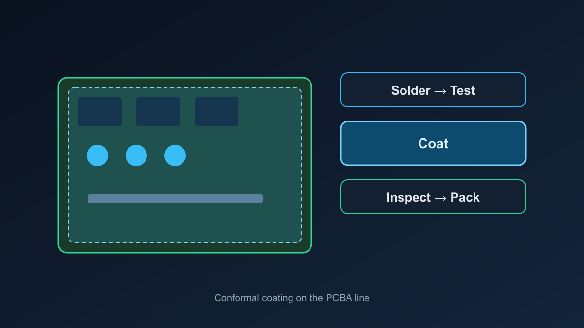
Where coating sits in the PCBA sequence
On a turnkey or consignment line, coating is a post-assembly protective step, not a fab process. A practical order looks like this:
- SMT (and through-hole / selective wave if needed)
- AOI / X-ray as drawn
- Cleaning if the flux or customer requires it before coat
- ICT and/or FCT before coat when fixtures contact pads, vias, or connectors that will be masked or covered
- Conformal coat: mask → apply → cure → UV / thickness inspect
- Post-coat electrical only when the drawing demands it (often limited fixtures or flying probe on exposed nets)
- Final pack with ESD and humidity controls suitable for a coated assembly
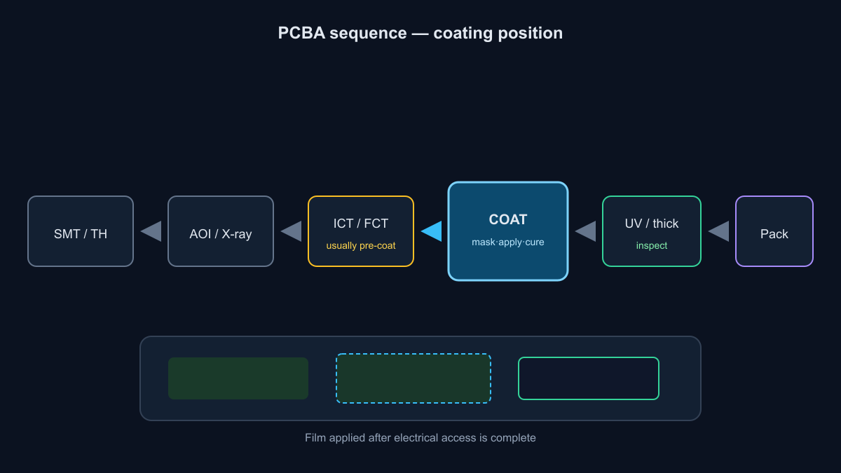
When ICT / FCT should run relative to coat
| Test type | Typical timing | Why |
|---|---|---|
| ICT with bed-of-nails on test pads / vias | Before coat | Coat film and keep-out masks block reliable nail contact; nails can also scar cured film |
| FCT through connectors / edge fingers | Before coat if those interfaces are keep-outs; after coat only with dedicated fixtures on uncoated points | Mating surfaces must stay clean and uncoated |
| Boundary scan / JTAG | Usually before coat | Same pad-access problem as ICT |
| Post-coat smoke / limited functional | After cure when risk of coat-induced shorts, opens, or leakage must be screened | Costly; only when product risk justifies it |
💡 Procurement Pro-Tip: Put the test-before-coat rule on the PO traveler, not only in a verbal kickoff. China PCBA houses default to whatever their last similar job did -- written sequence beats tribal memory.
If your design needs ICT after coat, you must design uncoated test lands and fixture strategy up front. Retrofitting that after first article is expensive.
Coating vs potting / encapsulation
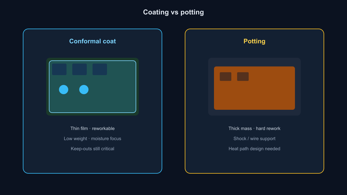
Conformal coating is a thin film that follows contours. Potting / encapsulation fills a cavity or covers a region with a thick polymer mass. They solve different mechanical and thermal problems.
| Factor | Conformal coating | Potting / encapsulation |
|---|---|---|
| Serviceability / rework | Often possible (chemistry-dependent) | Hard; usually destructive |
| Weight / volume | Low | High |
| Heat dissipation | Film adds little thermal mass; heatsinks still need keep-outs | Can trap heat; design for paths or thermally conductive fillers |
| Shock / vibration | Helps against moisture/chemicals more than structural shock | Better mechanical damping and wire-bond / part support |
| Cost / cycle time | Mask + spray/dip/CVD + cure; mid | Housing, mix, pour, long cure; often higher piece cost |
| Inspection | UV tracer + thickness samples common | Visual limited; voids hard to see without X-ray / section |
Choose coating when moisture, ionic leakage, and chemical splash are the drivers and you still want field or depot rework. Choose potting when shock, wire security, or cavity sealing dominate -- or combine: coat the board, pot a high-stress sub-region.
⚠️ Watch Out for: RFQs that say "waterproof coating" with no IP enclosure plan. A 25–75 µm film is not an IP67 gasket. Coating reduces condensation-driven leakage; it does not replace a sealed housing.
Process steps with buyer controls
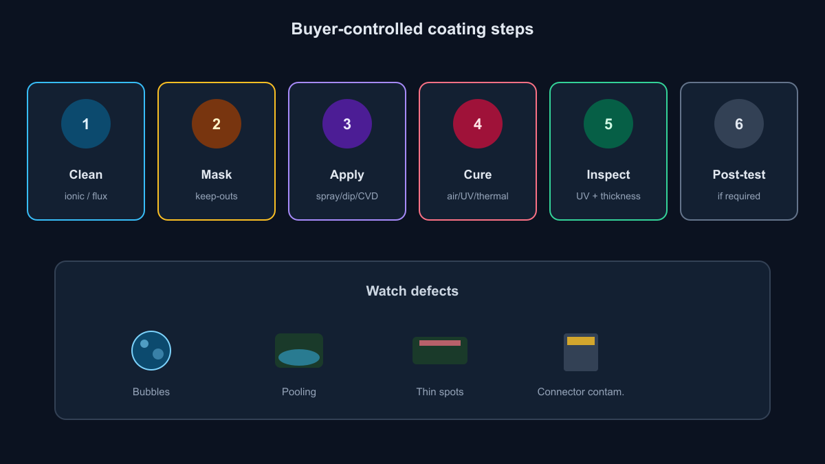
Treat the line as six commercial control points: clean → mask → apply → cure → inspect → post-coat electrical (if required).
1. Clean (ionic / flux)
Residue under the film becomes a moisture trap. Specify cleanliness method (aqueous, saponifier, solvent, plasma for special cases) and, when the product warrants it, ionic contamination limits or ROSE / ion chromatography sampling. No-clean flux still leaves residues that some chemistries dislike -- "no-clean" is not "no-clean-for-coat."
2. Mask keep-outs
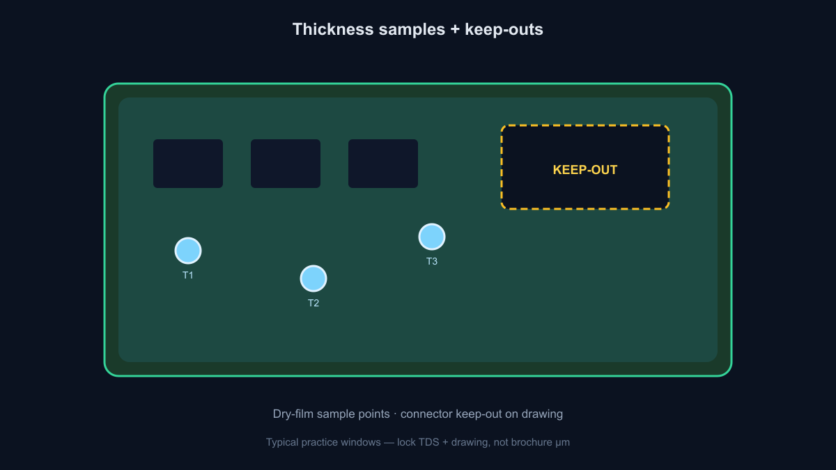
Masking is where most commercial disputes start. Lock a keep-out drawing: connectors, mating pins, screw lands, heatsink pads, RF shields that need metal contact, test points, adjustment pots, LED lenses, and any ground that must remain bare. Temporary masks (dots, tapes, boots, custom fixtures) must match that drawing. Permanent keep-outs belong on the fab/assembly drawing, not in a Slack thread.
3. Apply (selective spray / dip / brush / CVD)
| Method | Typical use | Buyer control |
|---|---|---|
| Selective spray | Mid–high volume, defined keep-outs | Program version, spray pattern, viscosity, edge definition |
| Dip | Simple boards, both sides | Withdrawal rate, drip time, edge beads |
| Brush / touch-up | Rework, low volume, selective zones | Operator skill; hard to audit -- limit scope |
| CVD (parylene) | Ultra-thin uniform XY films | Chamber load rules, masking quality, dimer lot |
Liquid systems are usually acrylic, silicone, urethane, or epoxy families. Parylene is vapor-deposited. Material family on the RFQ is fine; lock brand/grade only when the AVL requires it.
4. Cure (air / UV / thermal)
Follow the material TDS for solvent flash, UV dose, or thermal profile. Under-cure leaves soft film and solvent smell; over-cure can stress parts or embrittle some systems. Dual-cure (UV + moisture/thermal) materials need both legs completed -- UV-only "looks dry" is a common escape.
5. Inspect (UV + thickness)
Most liquid coatings carry a UV tracer. Specify UV coverage criteria (e.g., 100% visual UV on first article, then AQL or 100% by risk). Measure dry-film thickness on agreed coupons or board locations -- wet thickness alone is not acceptance. Watch common defects: bubbles, pooling in low spots, thin spots on tall component shoulders, and connector / pad contamination from mask failure.
6. Post-coat electrical (if required)
Only when the drawing says so. Scope it (full FCT vs limited continuity) and fixture rules so nails do not destroy the film.
💡 Procurement Pro-Tip: Ask for the keep-out drawing revision and the coating program ID on the CoC or traveler. If the factory cannot name both, thickness samples will not save a wrong-mask lot.
IPC-CC-830 myths -- material qualification ≠ board acceptance
IPC-CC-830 (including current C-series language buyers cite) is a qualification and quality conformance framework for conformal coating materials. It helps you compare candidate chemistries against standardized material tests. It does not, by itself, certify that your assembled board was coated correctly.
Acceptance of the coated PCBA still needs:
- Drawing callouts (chemistry family or AVL grade, sides, thickness window, keep-outs)
- Workmanship language where applicable (IPC-A-610 coating criteria as flowed down, plus customer visual standards)
- Process evidence (cure parameters, UV coverage, thickness sample plan)
- Customer-specific criteria (automotive, medical, industrial) when the program flows them
Saying "IPC-CC-830 coating" on a quote without a thickness window or keep-out map is marketing shorthand. Material CoC for the can of coating ≠ acceptance of the film on your serial number.
⚠️ Watch Out for: Certificates that only list an IPC-CC-830 material QPL-style claim and never mention dry-film thickness, sides coated, or UV inspection percent for your lot.
Thickness windows, keep-outs, and defects
Label the ranges below as typical industry practice, not legal limits. Always prefer the material TDS and your drawing.
| Chemistry family | Typical dry-film practice (order of magnitude) | Notes |
|---|---|---|
| Acrylic (AR) | ~25–75 µm common on many industrial boards | Easy rework; watch solvent sensitivity |
| Silicone (SR) | Often similar or slightly thicker windows | Soft surface; handling marks |
| Urethane (UR) | Often ~25–75+ µm depending on TDS | Tough; rework harder |
| Epoxy (ER) | Per TDS; often less rework-friendly | Brittle under flex |
| Parylene (XY) | Often much thinner uniform films (µm-class per TDS) | CVD process; masking critical |
Keep-out drawing as commercial control: thickness without keep-outs is incomplete. Edge definition at mask boundaries matters as much as mean thickness in the middle of a ground plane.
Common defects to name on the inspection plan:
- Bubbles / voids trapped in corners or under parts
- Pooling / bridging in low areas or between fine-pitch leads
- Thin spots on component tops and tall shoulders
- Mask leak → coating on connector pins or screw lands
- Orange peel / fisheyes from contamination
- Soft or tacky film from incomplete cure
China PCBA RFQ matrix for conformal coating
Paste this into the RFQ package so quotes are comparable:
| RFQ field | What to lock | Why it matters |
|---|---|---|
| Chemistry + brand/grade if locked | AR/SR/UR/ER/XY family; AVL P/N if required | Silent swaps change rework and environment fit |
| Dry-film thickness | Min/typ/max or TDS window + measure method | Wet mils alone are not acceptance |
| Sides coated | Top / bottom / both | Cycle time and mask cost |
| Keep-out map | Drawing rev with connectors, pads, heatsinks, TP | #1 dispute source |
| Cure method | Air / UV / thermal / dual | Under-cure escapes |
| UV inspect % | 100% FA + ongoing % or AQL | Coverage holes |
| Thickness sample plan | Locations, n per lot, instrument | Auditability |
| Post-coat test | None / limited / full FCT | Fixture damage risk |
| Lot / material CoC | Coating lot + board SN link | Traceability |
| Rework rules | Allowed strip chemistry; max cycles | Field and FA path |
| Packaging | ESD, humidity, separator sheets | Soft films scratch |
XFPCB can support PCBA builds that include conformal coating when chemistry family, thickness, keep-outs, and inspection language are on the drawing -- acrylic, silicone, urethane, epoxy, and parylene paths as the job requires. Share Gerbers, BOM, keep-out drawing, and test sequence for a DFM and process review. We do not invent "waterproof" claims the enclosure does not provide.
Soft close for buyers
If you are locking a China PCBA RFQ with coating, send the assembly drawing, keep-out layer, preferred chemistry family, dry-film window, and whether ICT/FCT runs before coat. XFPCB will map those fields to line capability and quote without swapping material families in silence.
Related XFPCB guides