
EAGLE CAD users lose schedule when the board “passes” in the editor but the zip China CAM opens is incomplete, mis-mapped, or sized to a rule deck that never matched the fab’s capability sheet. This guide is answer-first: schematic → board → placement and power/return → DRC against real fab windows → the exact Gerber/drill/BOM package fabs open → RFQ notes that cut EQ loops. It is not another EDA overview; for tool comparisons see PCB design software programs. Manufacturing handoff ownership: PCB design engineer role in manufacturing. DFM companion: PCB DFM.
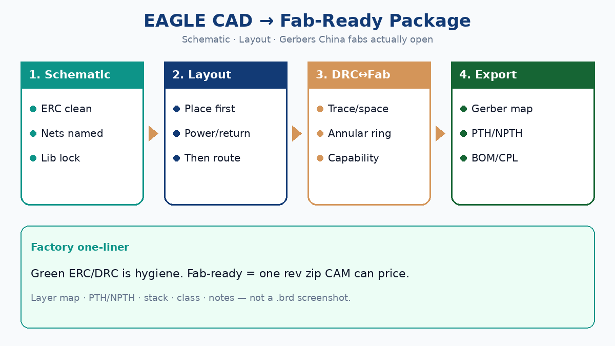
Answer first: the EAGLE release path that survives CAM
| Stage | What “done” means in EAGLE | What CAM needs from you |
|---|---|---|
| 1. Schematic lock | ERC clean; nets named; no floating pins you intend | Electrical intent is frozen before place |
| 2. Library / footprint lock | Package matches datasheet land pattern and courtyard | Pads and holes that plate and assemble |
| 3. Placement | Mechanical keepouts, connectors, thermal first | Geometry that can be routed and fabbed |
| 4. Power / return | Planes or pours before signal spaghetti | Continuous return; stitch vias where needed |
| 5. Route + DRC | Rule deck set to fab trace/space/annular ring | Green DRC against the fab window, not hope |
| 6. Export package | Gerber map, PTH/NPTH drill, notes, stack, BOM/CPL | One rev zip CAM opens without inventing defaults |
One-line definition: In EAGLE, fab-ready means the CAM desk can price and build from your zip without guessing layer order, hole plating, class, or stack. Green ERC/DRC alone is not a release package.
💡 Procurement Pro-Tip: Ask design for the layer map + PTH/NPTH note + IPC class in the same folder as Gerbers before RFQ. An
.brdscreenshot is not a fab package.
Process background: how PCBs are made. Buyer vocabulary: PCB terminology for buyers.
Footprint and datasheet lock before place
Most first-spin scrap from EAGLE shops is not “bad routing.” It is a wrong package placed early and never re-checked against the datasheet land pattern, pin-1 mark, and recommended pad sizes.
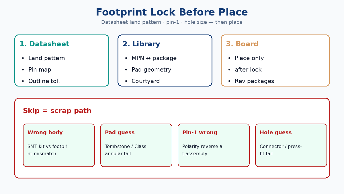
| Lock before place | Why it matters at China fab / SMT | Fail mode if skipped |
|---|---|---|
| MPN ↔ package | AVL and pick-and-place expect that body | Wrong footprint → scrap or hand rework |
| Land pattern vs datasheet | Pad size drives paste and annular ring | Tombstone, open, Class fail |
| Pin-1 / polarity | Silk and courtyard must match fab/assembly | Reverse polarity on diodes/ICs |
| Hole finished size | Drill + plate to finished ID | Press-fit wrong; connector won’t fit |
| Courtyard / keepout | DFM and assembly clearance | Collision after paste |
EAGLE habit: Treat the library part as a controlled document. If you edit pads for Class 3 or denser pitch, bump the package revision and re-run ERC/DRC. Do not “nudge pads on the board only” across five variants of the same MPN.
Datasheet check list (2 minutes per new package): recommended land pattern table, pin numbering diagram, package outline with tolerances, and any thermal pad / via-in-pad note. If the library came from a random internet ULPs dump, verify against the OEM PDF before place — especially for QFN, BGA, and fine-pitch connectors.
⚠️ Watch Out for: Mixing imperial library pads with metric fab notes, or using a “generic 0805” for a part whose datasheet wants a non-standard land. CAM will not fix your library; SMT will scrap it.
Placement before route; power and return first
Route-first in EAGLE produces nets that “connect” and boards that fail EMI, thermal, or yield. Place first. Pour and stitch power/return early. Signal routes last.
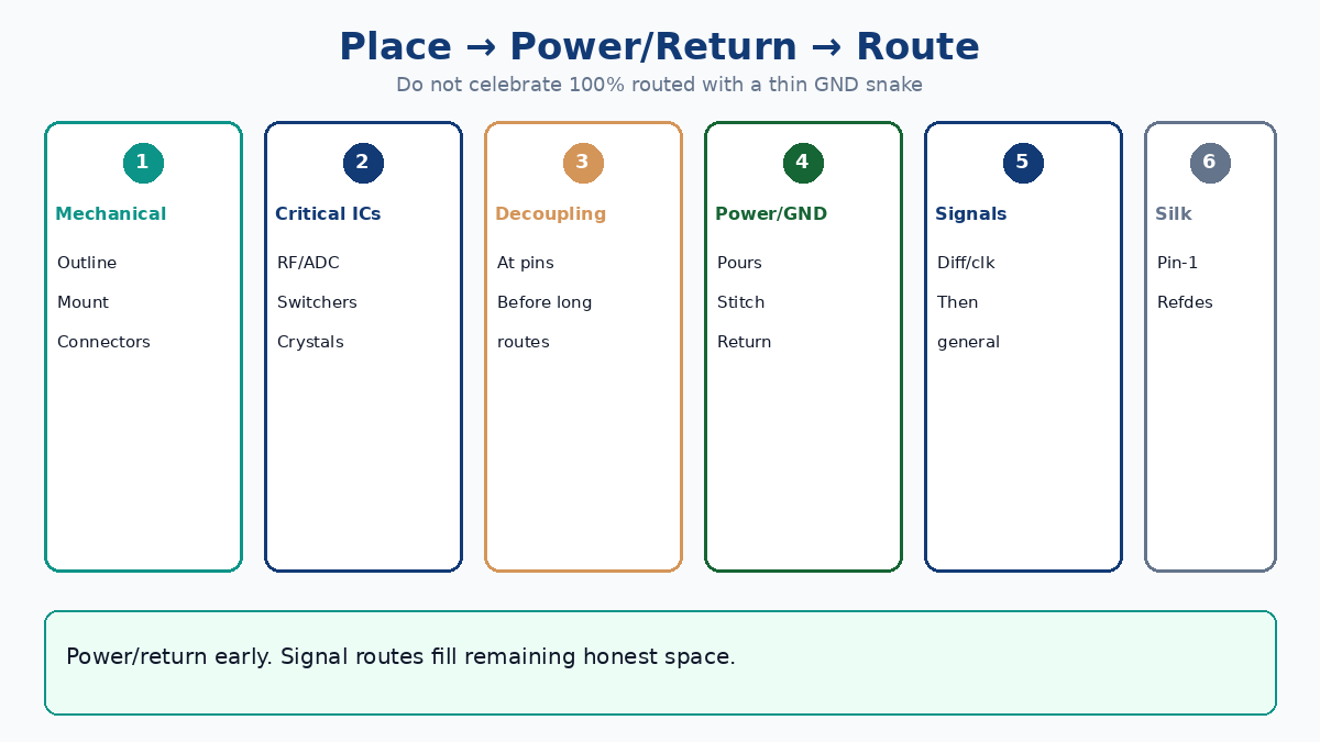
| Order | Focus in EAGLE | Factory reason |
|---|---|---|
| 1. Mechanical | Board outline, mounting holes, connectors, keepouts | Fab and enclosure do not move for copper |
| 2. Critical ICs | Crystal, RF, ADC, switchers near connectors they serve | Short sensitive paths; thermal headroom |
| 3. Decoupling | Caps next to power pins before long routes | Power integrity is placement, not hope |
| 4. Power / GND | Planes, pours, stitch vias, return under high di/dt | Continuous return reduces EQ on impedance / EMI |
| 5. Signals | Diff pairs, clocks, then general nets | Routing fills remaining space honestly |
| 6. Silk / mask | Pin-1, refdes away from paste and pads | Assembly and AOI readability |
Power/return rule: Do not celebrate “100% routed” if GND is a thin snake under a switching node. In EAGLE, create the copper pours and check islands before you declare DRC done. Stitch GND vias at connector shells, shield cans, and plane transitions.
Placement density tip: Leave fab-friendly channel for min trace/space from the capability sheet, not from the tutorial default. If your China fab’s standard is 5/5 mil and you place for 3/3, you either pay specialty pricing or get a DFM hold.
Related layout depth (tool-agnostic): use PCB DFM when placement forces copper closer than the plant window.
DRC vs China fab capability sheet
EAGLE DRC is only as good as the numbers you type. A green report against a hobby rule deck does not mean the board fits a China plant’s etch, drill, mask, and annular-ring window.
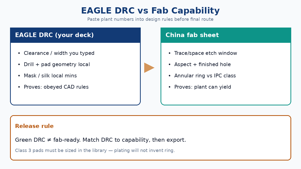
| Parameter | Put in EAGLE DRC / design rules | Match to fab capability sheet |
|---|---|---|
| Min trace / space | Clearance + width | Outer/inner etch window (e.g. 5/5 or 4/4 mil) |
| Min drill / finished hole | Drill size + pad | Aspect ratio and finished ID after plate |
| Annular ring | Pad − drill geometry | IPC class callout (Class 2 vs 3) |
| Solder mask dam | Mask stop / cream settings | Min dam between fine-pitch pads |
| Silk width / height | Legend rules | Fab min legend that survives |
| Copper to outline | Dimension / milling clearance | Route/V-score keepout |
Practical workflow: Paste the fab’s standard capability numbers into your EAGLE design rules before final route, not after Gerber export. Re-run DRC. Fix copper. Then export. If you need Class 3 annular ring, size pads for Class 3 in the library — do not hope plating “makes it.”
Green DRC ≠ fab-ready: DRC proves you obeyed your deck. DFM proves the plant can register, etch, plate, and yield. Treat fab DFM (or an early CAM review on dense multilayers) as the release gate. See PCB design engineer role for the traveler view.
💡 Procurement Pro-Tip: On the first China RFQ for a density step-up, require a written DFM (pass / conditional / fail) with the quote. Conditional DFM is where real cost and schedule hide.
Exact export package: Gerbers, drill, notes, BOM/CPL
China CAM desks open files. Ship one revisioned zip with a clear layer map. EAGLE’s CAM processor (or job file) should emit consistent extensions and a readme — not “whatever the last ULP named them.”
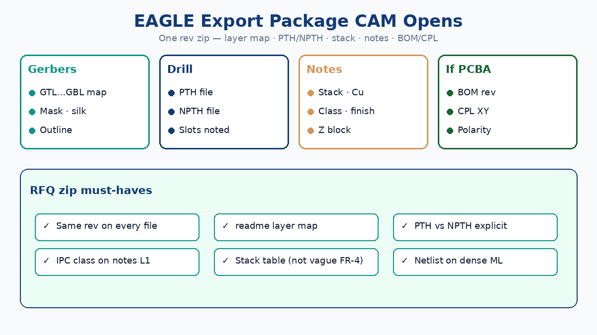
Gerber layer map (typical 4-layer example)
| Content | Common EAGLE / fab name | Notes CAM expects |
|---|---|---|
| Top copper | .GTL / Top Layer | Positive copper |
| Inner 1 / Inner 2 | .G2L / .G3L (or named inners) | Order matches stackup table |
| Bottom copper | .GBL | Mirrored correctly |
| Top / bottom soldermask | .GTS / .GBS | Expansion per notes |
| Top / bottom silk | .GTO / .GBO | No copper short under heavy silk |
| Board outline | .GKO / mill layer | Contour closed; units stated |
| Paste (if PCBA) | .GTP / .GBP | Stencil aperture intent |
Always include a one-page layer map in the zip (PDF or readme.txt): filename → layer function → polarity. Units (inch/mm) and coordinate origin must match drill.
NC drill: PTH vs NPTH
| File | Contents | Callout |
|---|---|---|
| PTH drill | Plated holes / vias | Finished size after plate; tolerance |
| NPTH drill | Unplated (mounting, tooling) | Explicit NPTH — never “assume” |
| Slot / mill | Plated or unplated slots | Separate note if not in drill |
EAGLE users often export one Excellon file with mixed plating intent. Split PTH and NPTH (or document plating in a hole chart). Ambiguous NPTH that gets plated is a classic China EQ and fit failure on mounting holes.
Fab notes + stackup (minimum)
| Block | Must state |
|---|---|
| Stackup | Layer count, Cu oz, thickness, Tg / material family |
| Finish | HASL / ENIG / etc. |
| Mask / silk | Color; via tent/open/plug if required |
| IPC class | Class 2 or Class 3 on line 1 of notes |
| Impedance (if any) | Z0/Zdiff, layer, tolerance, coupon yes/no |
| Rev | Single rev letter for all files |
BOM / CPL if PCBA
| Deliverable | “Done” looks like |
|---|---|
| BOM | MPN, qty, refdes, DNP flags, same rev as Gerbers |
| CPL / centroid | XY, rotation, side, matching refdes |
| Polarity notes | Pin-1 / cathode callouts for ambiguous packages |
⚠️ Watch Out for: Shipping Gerbers from rev B and a BOM from rev A, or a single drill file with no PTH/NPTH note. CAM will stop or price the expensive safe guess.
RFQ checklist for EAGLE users sending to China fab
Use this as the email/attachment checklist. Soft CTA: XFPCB quotes from drawing-driven packages — stackup, class, and layer map on the traveler — not from .brd screenshots.
| # | Item | Pass criterion |
|---|---|---|
| 1 | One zip, one rev | All Gerbers + drill + notes share the same rev letter |
| 2 | Layer map | Filename → function table in readme/PDF |
| 3 | PTH / NPTH | Separate files or explicit hole chart |
| 4 | Stackup table | Cu, thickness, material/Tg — not “FR-4 equivalent” only |
| 5 | IPC class + finish | On fab notes line 1 |
| 6 | DRC vs fab sheet | Min trace/space/annular ring match quoted capability |
| 7 | Netlist (IPC-356) | Attached for copper compare on dense boards |
| 8 | Impedance block | If controlled Z: targets, layers, coupon/TDR yes-no |
| 9 | BOM + CPL | Only if PCBA; rev-matched |
| 10 | Contact for EQ | Single engineer email; answers as drawing deltas |
EQ cuts that work: freeze class and stack before RFQ; put NPTH in writing; answer CAM with note numbers, not chat paragraphs. Most multi-day holds on EAGLE jobs are blank class, mixed revs, and undivided drill plating intent.
Soft next step: If you are releasing a multilayer or PCBA job from EAGLE to China, attach the layer map, PTH/NPTH note, and class/stack locks with the first RFQ. Pair this workflow with PCB design software programs (tool landscape), design engineer manufacturing role (handoff ownership), PCB DFM, how PCBs are made, and PCB terminology for buyers.