
Electro-deposited (ED) copper foil is still the default conductor on rigid multilayer PCBs. It grows on a rotating drum, so one face is shiny (drum contact) and the other is matte (growing grains). After electroforming, mills add surface treatments — nodular, barrier, passivation, and often silane — before the foil becomes CCL. Write only "1 oz copper" and CAM ships whatever grade and treatment laminate stock carries. This factory note covers drum manufacture, the four treatments, Grade 1 vs Grade 3/HTE RFQ language, and the peel vs etch/impedance tradeoff. ED-versus-RA selection and HTE-versus-low-roughness yield live in separate XFPCB materials guides.
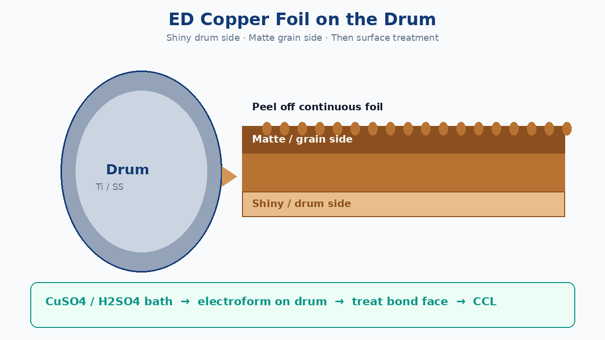
How ED foil is made on the drum
Copper is dissolved into a copper sulfate–sulfuric acid bath, cleaned up, then plated onto a rotating stainless or titanium drum. Thickness builds with current density, bath chemistry, and drum speed. The continuous sheet peels off the drum as foil.
That geometry locks two faces:
| Face | How it forms | What CAM/laminators care about |
|---|---|---|
| Shiny side (drum side) | Copper against the polished drum | Smooth start surface; often the outer face before treatment stack |
| Matte side (grain side) | Free growth into the bath | Natural roughness from copper crystallites; usual bond face after nodular treatment |
Grain structure, tensile strength, and elongation move when the mill changes bath additives, current, and temperature. That is why two foils with the same ounce weight can behave differently under lamination and reflow — weight alone never tells the full story. IPC-4562 is the shared metal-foil vocabulary (Type E for ED, grades, profile language). Buyers do not need to recite tables; they need the grade and treatment intent on the drawing.
💡 Procurement tip: On multilayer RFQs, ask which face of the starting foil bonds to the dielectric on each critical layer. "ED copper" without face/treatment language still leaves peel and etch geometry to the mill default.
Why foil gets treated after electroforming
Bare ED foil oxidizes in storage, bonds poorly to many resins, and can lose interface strength when heat and chemistry hit during lamination or assembly. Surface treatment is not cosmetic branding. It is a thin engineered stack that:
- Raises mechanical interlock and chemical adhesion to the resin
- Protects the copper–resin interface under thermal stress
- Slows oxidation so rolls survive shipping and layup
- In some high-performance laminates, improves coupling to the resin system and glass cloth
Untreated foil is a lab curiosity for most rigid multilayer jobs. What arrives on CCL is treated ED — and the treatment choices change peel, etch undercut, and high-frequency loss. Specifying ounce weight and ignoring treatment is how SI models and travelers diverge.
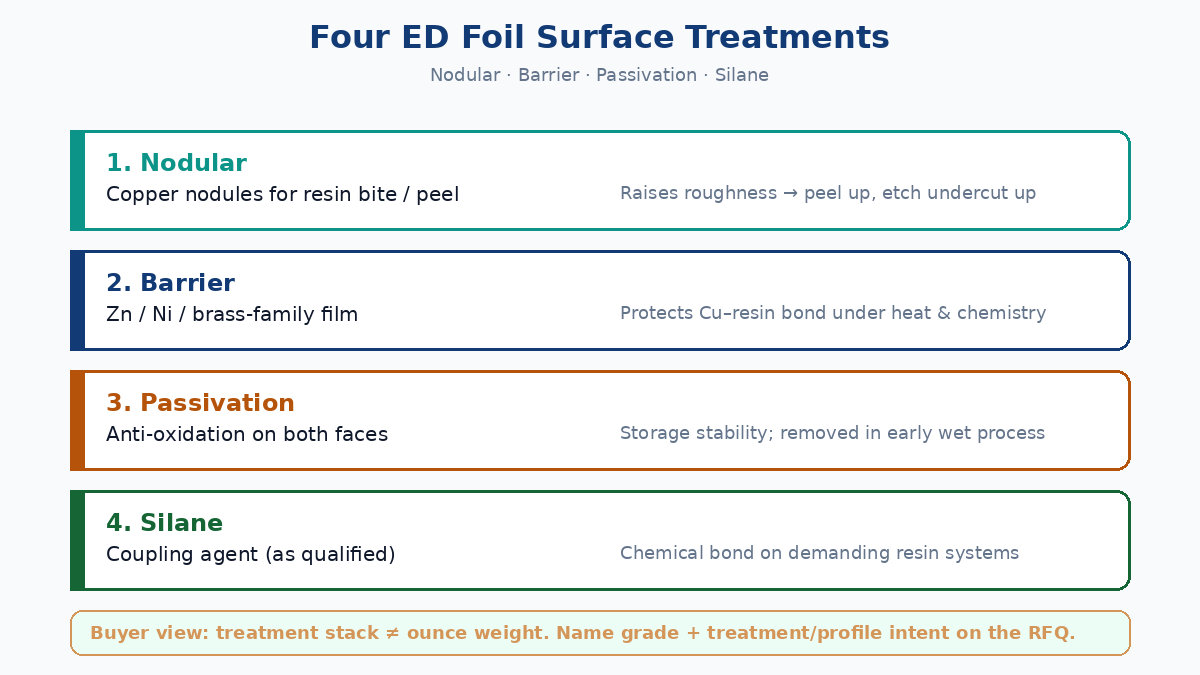
Four surface treatments buyers should recognize
Mills apply these in sequence after electroforming. Exact chemistry and thickness sit with the foil maker and laminate qualification; the buyer-facing map is what each step is for.
1. Nodular treatment
Copper nodules (sometimes oxide-assisted morphologies) are plated onto the bond face to increase surface area and resin bite. The layer is thin relative to foil thickness, but it drives peel on commodity FR-4 as well as tougher systems such as polyimide, BT, and cyanate ester.
More nodule aggressiveness usually means higher peel — and more etch undercut, slower etch, and more conductor roughness for skin-effect loss. That is the same peel-versus-geometry tension discussed later; nodular treatment is where much of that roughness is created, not an accident of the drum alone.
2. Barrier layer
A thin zinc, nickel, or brass-family coating sits over the nodular structure. Its job is to protect the copper–resin bond during heat and chemical exposure in lamination and assembly — not to thicken the conductor for current carrying.
Color on foil samples can look brown, grey, or mustard depending on metal mix. Thickness is measured in angstroms-class films, not copper ounces. Buyers rarely call a barrier alloy by name on commercial RFQs; they feel barrier quality as peel retention after thermal stress, not as a Gerber field.
3. Passivation / anti-oxidation
Both faces typically receive a chromate-style or organic anti-oxidation film so rolls do not green up in humidity before layup. These films sit under roughly angstrom-scale thickness and come off early in PCB wet processes (clean, scrub, etch).
If passivation is weak or storage is long and wet, oxide can still appear before imaging. That is a receiving/handling problem more than a design-rule problem — but oxidized foil that enters layup dirty is a delamination and etch-uniformity risk.
4. Silane (coupling agent)
Silane-based coupling agents improve chemical bonding between treated copper and the resin system and help resist contamination. On some high-performance constructions they also support bonding near glass reinforcement.
Silane shows up most when the laminate family is picky (high-Tg, low-Dk, PI/BT-class). On commodity FR-4 with standard nodular treatment, buyers seldom need a separate silane callout — the mill's qualified stack already includes whatever coupling the slash sheet needs. When you change resin family, ask which foil treatment is qualified on that datasheet, not only which profile code is cheapest.
| Treatment | Primary purpose | Buyer-facing risk if ignored |
|---|---|---|
| Nodular | Peel / resin interlock | Low peel or excess tooth for fine line |
| Barrier | Protect bond under heat/chemistry | Peel drop after press or reflow |
| Passivation | Storage oxidation control | Oxide, dirty layup, uneven etch start |
| Silane | Chemical coupling on demanding resins | Delam or weak bond on high-perf systems |
Grade 1 vs Grade 3 / HTE — RFQ language that sticks
IPC-4562 Grade 1 is standard ED foil for many single-sided and simple multilayer jobs. Grade 3 is High Temperature Elongation (HTE): the foil is formulated to keep useful ductility when the board is hot — lamination presses and lead-free reflow — not only at room-temperature tensile numbers.
During heat, dielectrics expand in Z. That motion loads copper near plated through holes. Foil that goes brittle at temperature cracks or separates; HTE is meant to absorb more of that strain. That is why Grade 3 / HTE is the usual multilayer default in China fab practice when drawings are silent but builds are thick or reflow-heavy — and why Grade 1 on a thick MLB is a reliability gamble, not a free cost save.
RFQ phrases that CAM can enforce:
- "Inner/outer start copper: ED, IPC-4562 Grade 3 (HTE). Grade 1 not acceptable on multilayer."
- "HTE Grade 3 on all copper layers; profile/treatment per laminate datasheet unless Rz capped below."
- "Single-sided / simple 2-layer consumer: Grade 1 ED acceptable unless drawing says HTE."
Phrases that do not stick:
- "High quality copper" / "good elongation" with no grade
- "1 oz copper" alone on a thick MLB or multi-reflow stack
- Assuming AS9100 or "aerospace fab" implies HTE without a foil grade callout
XFPCB already publishes a deeper factory note on HTE Grade 3 versus low-roughness foil for fine-line yield and PTH crack risk. Use that when the fight is ductility versus VLP/RTF tooth height. This article stops at grade language so the RFQ names Grade 1 or Grade 3 before profile debates start.
⚠️ Watch out: Mixing "HTE" marketing with Grade 1 stock. If the PO does not say Grade 3 / HTE, a quiet Grade 1 pull on a thick stack is hard to catch until microsection or IST. Put the grade next to ounce weight on the stackup table.
Peel strength vs etch accuracy and impedance
Nodular roughness that helps peel also hurts geometry:
- Longer etch time and more lateral undercut (weaker etch factor)
- Trace edges that no longer match the rectangle in the SI model
- Local dielectric thickness scatter when teeth bite thin cores
- At higher frequency, skin effect rides the rough surface and conductor loss rises
So the same treatment stack that makes a laminate "peel safe" can make fine-line etch and controlled impedance harder. Low-profile / reverse-treated families dial tooth down for HF and HDI; peel usually drops versus standard-tooth HTE on the same resin. That is a deliberate trade, not scrap.
Buyer decision rule (shop-practical):
- Wide lines, peel and thermal reliability first, frequency comfortable → standard-treated HTE Grade 3 is usually enough.
- Fine inner L/S or impedance on thin dielectric → cap roughness (VLP/RTF language or Rz on the bond face) and keep Grade 3 if the stack is multilayer.
- High-perf resin (PI/BT/low-Dk) → confirm foil treatment qualification on that slash sheet; do not assume FR-4 nodular chemistry transfers.
Do not invent Rz numbers on the RFQ unless your SI model and laminate datasheet agree. Prefer named profile families the fab stocks (STD / LP / VLP / RTF) plus Grade 3, then ask CAM to confirm peel on the named core. XFPCB's copper foil overview covers ED vs RA and the VLP/HVLP/RTF ladder in more depth when the question is foil type rather than treatment stack.
Fab notes and RFQ lines that prevent silent defaults
Incomplete foil notes become stock Grade and stock tooth. Complete ones are short and sit beside the stackup.
Minimum that prevents the wrong grade and the wrong tooth:
- Process: ED (Type E)
- Grade: Grade 1 or Grade 3 / HTE — explicitly
- Weight per layer or zone
- Profile or Rz intent on critical faces (or "treatment per laminate datasheet" when defaults are acceptable)
- Resin family note when leaving commodity FR-4
CAM-ready example language (adapt to your stack):
- All inner signal layers: ED HTE Grade 3, start weight as stacked; profile VLP or RTF equivalent on impedance layers; planes may use standard-tooth HTE if peel is the priority.
- Outer start copper: ED HTE Grade 3 unless the outer is not reliability-critical and Grade 1 is written on purpose.
- No Grade 1 substitution on multilayer without written EQ approval.
Avoid locking a single foil brand with no equivalent when lead time matters. Avoid demanding maximum peel and minimum roughness in the same sentence with no trade accepted. Avoid "smooth copper" without a profile or Rz vocabulary CAM shares.
When grade, ounce weight, and treatment/profile intent sit on the same sheet as the stackup, XFPCB CAM can match laminate stock, flag indent low-roughness foils, and refuse quiet Grade 1 or STD-tooth swaps. That is how drum-side physics, treatment chemistry, and RFQ language stop fighting on the traveler.
For quote review on multilayer or HF builds, send Gerbers, stackup table, and foil callouts together through the XFPCB how-to-place-an-order flow so CAM sees grade and treatment before pricing defaults.
Related XFPCB guides
- PCB Copper Foil: ED vs RA, Low-Profile Choices, and What to Put on Fab Notes
- HTE and Low-Roughness Copper Foil for High-Density PCBs: Reliability vs Fine-Line Yield