
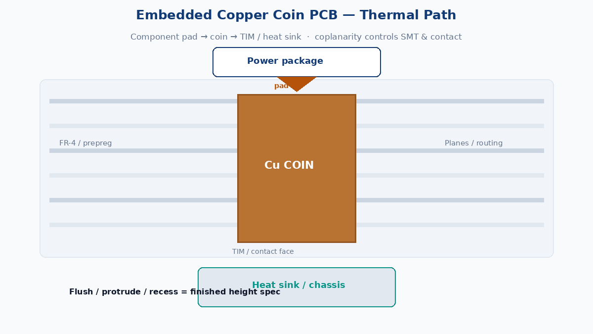
An embedded copper coin PCB is a multilayer board with a solid copper insert under a high-heat package. The coin is a localized thermal bridge — pad → coin → TIM / heat sink or chassis — not a cooling system by itself. Buyers pick it when thermal vias or heavy copper cannot clear a concentrated hotspot without eating routing. Yield hinges on cavity clearance, resin fill, finished flush/protrude/recess height, and coplanarity that SMT and heat-sink contact can actually live with.
Answer first: what it is, how made, thermal + DFM
| Question | Factory / procurement answer |
|---|---|
| What is a copper coin PCB? | Multilayer PCB with a solid copper block embedded (or press-fit) under a hotspot — continuous metal path, not foil ounces |
| How is it made? | Define coin in stack-up → machine coin + cavity → clean/treat coin → fixture → laminate-embed or press-fit after laminate → planarize → form layer connections |
| Thermal design? | Full path: package → solder/TIM → coin → bottom TIM → sink/chassis. Coin cuts resin out of the vertical path; sink and pressure still decide the end temperature |
| Why DFM early? | Cavity clearance, resin content, coplanarity, and net/plating must match one drawing set before CAM quotes |
| Fear list (implicit) | Delamination, resin voids, flush resin on the coin face, coplanarity that tilts packages or opens TIM gaps |
💡 Procurement tip: Put coin dims, cavity clearance, finished height (flush / protrude / recess), connected net, plating intent, and coplanarity on the RFQ — not only “add copper coin under U3.” Silent fields become fab defaults.
Structures and terminology (name each axis)
Callouts on drawings often mix shape, depth, install method, and electrical role. Split them:
| Axis | Typical language | What CAM needs |
|---|---|---|
| Embedding depth | Through, partial-depth, fully buried | Which layers the coin spans; exposed top/bottom faces |
| Geometry | I-Coin, T-Coin, H-Coin, stepped / custom | Machining envelope + land/tab geometry |
| Installation | Laminated embedded, press-fit, plated-in | Process traveler — not interchangeable line items |
| Electrical | Connected, partial, isolated | Net name, clearances, wall plating yes/no |
A T-Coin is a shape. Press-fit is an install method. Writing both in one blurry note is how quotes and travelers diverge.
Thermal path — bridge, not the sink
Typical path:
Component thermal pad → solder joint or TIM → copper coin → bottom TIM / contact → heat sink, chassis, or cold plate
Solid copper shortens the vertical path through low-conductivity resin and laminate. The coin may also tie to planes for lateral spreading or carry localized high current / ground. Final performance still depends on package thermal resistance, joint quality, coin contact area, TIM thickness, sink flatness, mounting pressure, and airflow or liquid cooling. Do not treat the coin as a standalone °C/W promise — system path wins or loses.
Manufacturing steps (laminated vs press-fit diverge mid-flow)
1. Define the coin in the stack-up
Same structure in stack-up table, mechanical drawing, Gerber/ODB++, and fab notes:
- Shape, XY size, thickness / layer span
- Exposed faces and finished flush / protrude / recess
- Electrical net (or isolated)
- Cooling interface (top package pad, bottom sink pad, both)
2. Machine coin and cavity as a matched pair
Cylindrical, rectangular, T/H, stepped, or custom. Openings in cores, prepregs, foils, or the laminated board must allow for coin tolerance, routing tolerance, resin-flow space, placement clearance, tool corner radius, plating buildup, and (for press-fit) interference. Nominal coin = cavity is a scrap recipe.
3. Prepare the coin surface
Oil, oxide, and shop dirt kill wetting. Clean, micro-etch, or other fab-approved roughening before embed/insert so resin or plating can bond.
4. Position and fixture
Hold X-Y, height, tilt, and registration to internal copper. Drift shows up as thermal-pad offset, clearance violations, coplanarity scrap, and uneven resin around the perimeter.
5. Laminate-embed or press-fit insert
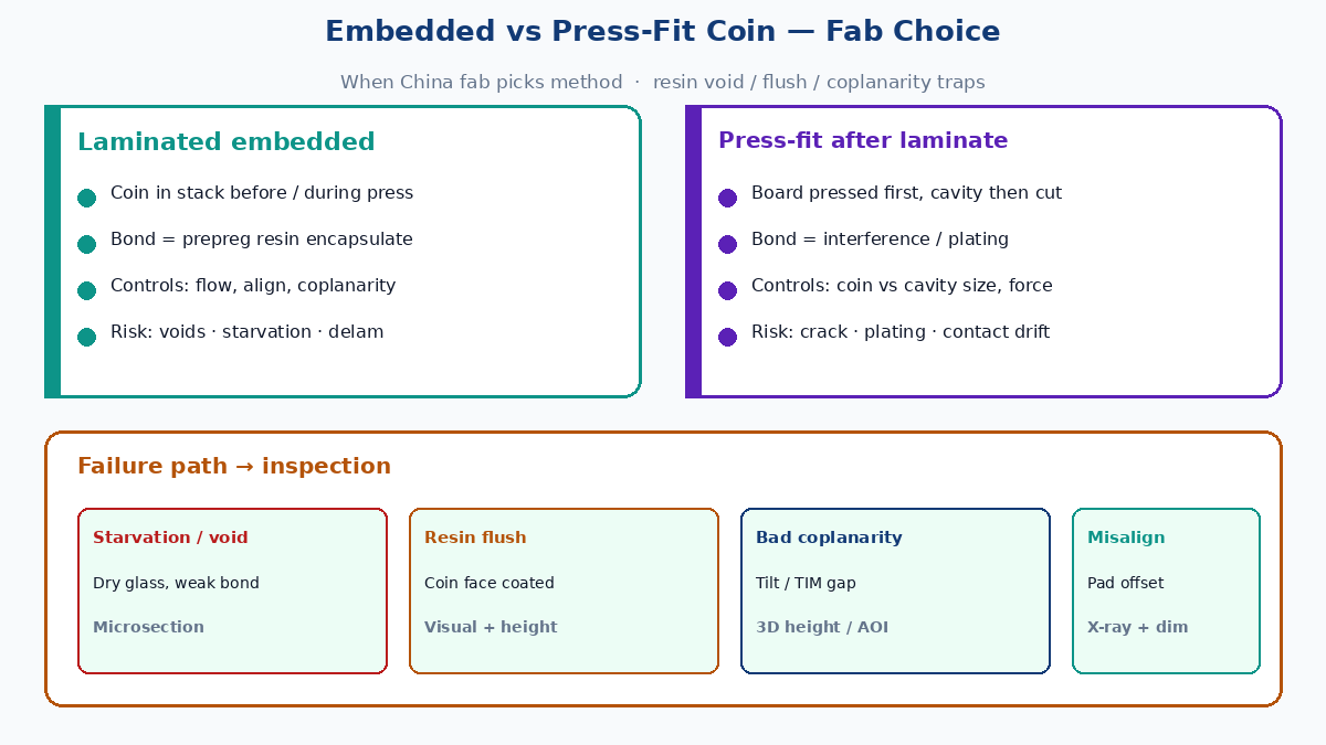
- Laminated embedded: coin in the stack before or during press; heated prepreg flows and cures around it.
- Press-fit: board laminated first; cavity machined; coin forced in; retention by interference and/or metallization.
Different cavity sizes, travelers, connection schemes, and inspection plans.
6. Remove resin flush and planarize
Resin on the exposed coin face is common after press. Controlled grind/sand sets finished board thickness and coin height. Call the finished condition explicitly — flush, protruding, or recessed.
7. Form layer connections
Surface copper, internal lands/tabs, cavity- or slot-wall plating, plated-in structures, or mechanical contact (press-fit). Drawing must name connected layers, geometry, and clearances.
Resin fill and cavity clearance
Resin mechanically supports the coin–laminate interface. The copper body remains the thermal path; resin is bond and dielectric fill, not the heat pipe.
| Clearance condition | What goes wrong |
|---|---|
| Too tight | Hard insertion, blocked flow, local dry spots |
| Too loose | Excess resin demand, coin shift, height scatter |
| Uneven | Resin-rich vs starved zones, asymmetric stress |
| Locally enclosed | Trapped air → lamination voids |
No universal gap. Geometry, thickness, prepreg system, install method, and wall-plating rules set the window. Prepreg resin content, glass style, adjacent copper density, press profile, and tooling all change flow around a large copper mass that locally rewrites pressure.
Starvation, flush, voids — failure path
- Resin starvation → dry glass, incomplete wrap, weak bond → delam risk in reflow / thermal cycle.
- Resin flush → cured resin film on the coin face → planarize harder; soldering or TIM contact degraded if flush remains.
- Voids → trapped air / poor wet / blocked flow → higher local thermal resistance + crack starters.
Inspection split: X-ray finds position and large gaps. Microsection judges fill quality, interface separation, wall plating, and fine cracks. Visual + 3D height catch flush and finished height. High-rel builds may add reflow sim or thermal/power cycle — agree criteria on the PO, do not invent numbers in marketing copy.
Coplanarity — finished-board requirement
Finished coin may sit flush, proud, or recessed relative to the surrounding laminate.
| Coin height | Assembly / thermal trap |
|---|---|
| Protruding | Package tilt, uneven joints, sink rocker / over-pressure |
| Recessed | Extra solder or TIM thickness, weak thermal contact |
| Assumed from nominal thickness | Ignores prepreg crush, resin flow, and planarize — scrap after stencil |
Specify coplanarity (or max protrude/recess) as a finished requirement. SMT paste, TIM bond-line, and heat-sink flatness all ride that number.
⚠️ Assembly trap: A coin that passes bare-board visual can still kill SMT if coplanarity was never on the fab drawing. Lock TIM thickness window and sink mounting with the same height callout used for planarize.
Layer connections and plating risks
Coins may land on a package thermal pad, power/ground planes, and/or an external cooling face. Internal ties use lands, tabs, direct interfaces, or plated cavity/slot walls.
Plated-in / slot-wall risks: incomplete plate, misalignment, corner cracking, contact resistance climb after thermal cycle. Continuity test + microsection (and cycle where required) beat hope.
Embedded vs press-fit — when China fab chooses
| Laminated embedded | Press-fit after laminate | |
|---|---|---|
| Stage | Before / during press | After press + cavity machine |
| Fixing | Prepreg encapsulation | Interference and/or metallization |
| Main controls | Resin flow, alignment, coplanarity | Coin vs cavity size, insertion force |
| Layer connect | Designed Cu interface or plating | Plated wall or mechanical contact |
| Main risks | Voids, starvation, delamination | Cracking, plating damage, unstable contact |
Fab choice pattern (qualitative): laminated embed when the coin is designed into the stack early and resin bond + planarize are qualified; press-fit when the plant wants a finished core first, or when cavity machining after laminate fits the traveler. Do not swap methods mid-quote without reopening cavity dims, plating, and inspection.
When a coin beats vias / heavy copper / MCPCB
| Approach | Strength | When coin usually wins |
|---|---|---|
| Thermal via array | Cheap vertical paths | Coin wins on concentrated high heat-flux under one pad when via count would steal routing or still leave resin in the path |
| Copper-filled vias | Solid vertical plugs | Mid hotspots / via-in-pad; coin when one continuous mass under the package is simpler than a via forest |
| Heavy copper | Lateral spreading + current | Distributed heat / high amp traces; coin when the need is a local vertical bridge |
| Metal-core PCB (MCPCB) | Board-wide metal base | Distributed board-level heat; coin when multilayer routing density must stay and only one zone needs metal |
Coin = localized continuous vertical path while keeping multilayer routing. MCPCB = broad conduction into a metal base. Heavy copper = mostly lateral. Vias = discrete verticals. Pick from the heat map and routing budget, not from a catalog slogan. No invented thermal-resistance numbers — compare paths and DFM cost on the actual stack.
DFM checklist — electrical, mechanical, assembly
Electrical
- Coin net (or isolated)
- Connected vs kept-out layers
- Inner connection geometry
- Cavity/slot-wall plating yes/no
- Clearances to signal, RF, and vias
Keep large coins off critical return paths unless the SI owner signed off.
Mechanical / stack-up
- Coin dims + layer span
- Cavity dims + clearance
- Position tolerance
- Finished protrude / recess + coplanarity
- Stack symmetry and copper balance (warpage)
Assembly / thermal
- Package thermal-pad design and paste aperture
- TIM thickness window
- Heat-sink flatness and mounting pressure
- Reflow / rework exposure the interface must survive
Have the fab approve coin dims, cavity tolerances, and coplanarity before the fab drawing freezes.
Stress, reliability, defects
Stress concentrates at coin corners, resin interfaces, plated walls, and nearby vias. Reflow, rework, and thermal cycling expose weak fill and bad plating.
| Defect | Impact | Preferred check |
|---|---|---|
| Coin misalignment | Pad offset / clearance hit | Dimensional + X-ray |
| Starvation / voids | Weak bond, higher local thermal resistance | Microsection |
| Resin flush / wrong height | Solder or TIM problems | Visual + 3D height |
| Slot-wall crack | Unstable electrical path | Microsection + continuity |
| Interface separation | Delam after cycle | Microsection + cycle (if required) |
| Board warpage | SMT and mechanical assembly scrap | Bow/twist |
Risk rises with oversized or asymmetric coins, incomplete fill, loose coplanarity, and unbalanced stacks.
China fab RFQ fields for copper coin (copy into the PO)
Minimum set that prevents silent defaults:
- Coin dims — XY, thickness / layer span, geometry family (I/T/H/stepped/custom)
- Cavity clearance — matched system with install method (embed vs press-fit)
- Finished height — flush / protrude / recess + coplanarity limit
- Net — connected layers or electrically isolated
- Plating — cavity/slot-wall plating intent and acceptance
- Inspection — X-ray for position; microsection for fill/plating sample plan
- Assembly note — TIM / sink coplanarity dependency if XFPCB or CM builds PCBA
Incomplete notes become “whatever cavity the router cut last week.” Complete notes are short and sit beside the stack-up table.
Bottom line: An embedded copper coin PCB earns its keep on concentrated hotspots that vias, heavy copper, or MCPCB handle poorly. Performance is the full thermal path; reliability is resin fill, coplanarity, and connection integrity. Review the coin with the fab before the stack-up and fab drawing lock — after first article is the expensive time to discover voids and tilt.