
Board warpage — bow and twist that keep a PCB from sitting flat — is one of the fastest ways a “good” fab lot becomes an SMT yield problem. Overseas buyers and engineers usually search causes, IPC-style limits, and prevention after a BGA run shows opens, head-in-pillow, or coplanarity scrap. This page is that factory checklist: what bow vs twist means on the traveler, how commonly referenced % of diagonal limits are used as buyer guidance (confirm with your fab and latest IPC edition), what drives warpage through stackup/copper balance, moisture/bake, and reflow support, how to measure and write RFQ language, and which levers actually move fab+SMT yield. It is not a laminate CTE / registration theory article; that lives on the dimensional-stability guide. Here the job is flatness for assembly.
Quick answer: keep boards flat for SMT
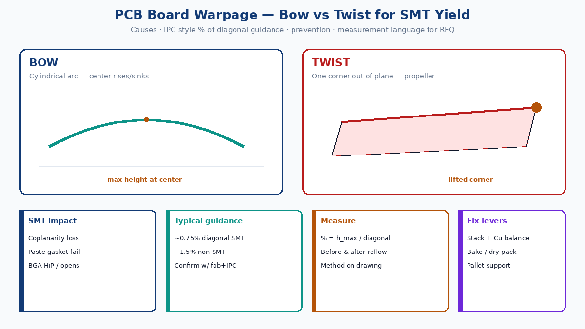
- Name the defect — bow (cylindrical arc) vs twist (one corner out of plane). Both are warpage; diagnosis differs.
- State a limit on the drawing — buyers often reference roughly ≤0.75% of diagonal for SMT and a looser figure for non-SMT as typical industry guidance. Confirm the exact acceptance with your fab/assembly house and the latest IPC edition you contract to.
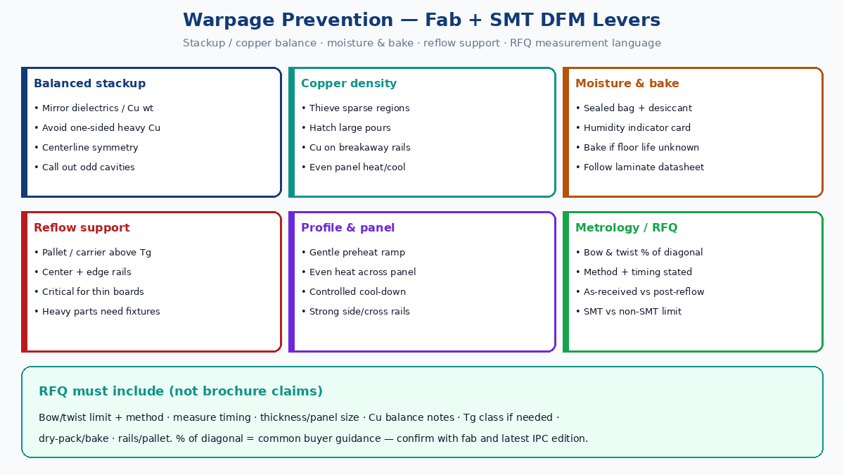
- Balance the stack — mirror dielectric and copper weights about the centerline; fix large one-sided pours with thieving or hatch.
- Control moisture — sealed pack, desiccant, humidity cards; bake when exposure history is unknown before lead-free reflow.
- Support above Tg — rails, pallets, and center supports so the panel does not sag when the resin softens.
- Measure before and after reflow — separates fab-intrinsic warp from assembly-induced sag.
💡 Factory gain: Put bow/twist method (diagonal length, max height, %), measurement timing (as-received / post-bake / post-reflow), and SMT vs non-SMT acceptance on the fab drawing. “Meet IPC” without numbers is how two plants both pass paperwork and still scrap BGAs.
Bow vs twist: what you are rejecting
| Shape | Geometry | Typical SMT symptom |
|---|---|---|
| Bow | Board curves as an arc; corners tend to stay in one plane while the center rises or sinks | Center BGAs lose coplanarity; paste transfer uneven across a large QFP |
| Twist | One corner lifts relative to the other three (propeller) | Corner connectors and edge BGAs rock; stencil gasketing fails on one side |
Warpage is out-of-plane deformation from residual and thermal stress. Copper, glass, and resin expand and contract at different rates. If the stack or copper density is asymmetric, the board bends toward the side that shrinks more on cool-down. Thin boards (about 0.8 mm and below), large panels, heavy copper on one face, and double-sided reflow make that mismatch visible on the line.
Commonly referenced limits (buyer guidance — confirm)
Industry RFQs and traveler notes frequently cite bow/twist as a percentage of the board diagonal:
- SMT assemblies: often referenced around 0.75% of diagonal
- Non-SMT / through-hole heavy builds: often referenced around 1.5% of diagonal
Example math: diagonal 300 mm → 0.75% ≈ 2.25 mm max height at the worst point under the stated method.
Treat these as commonly referenced buyer planning numbers, not a silent guarantee that every fab lot will hit them without a drawing callout. Always:
- Name the measurement method (flat plate + feeler / dial indicator / optical scan).
- State when you measure (bare board as shipped, after bake, after first reflow).
- Confirm against the fab capability sheet and the IPC edition named on the PO.
- Tighten further for large BGAs, fine-pitch connectors, or press-fit cages if your assembly house requires it.
Do not invent tighter “factory capability” claims in marketing language. Put the number you will reject to on the drawing.
Why boards warp (fab + assembly)
Asymmetric stackup
Dielectric thickness, copper weight, or resin content that is not mirrored top-to-bottom builds a bimaterial strip. Lamination cool-down and reflow both amplify it. Cavities, odd-layer counts without a clear center plane, and one-sided heavy copper are classic offenders.
Uneven copper distribution
Large solid planes opposite sparse routing heat and cool differently. Local stiffness and shrinkage differ, so the panel bows toward the copper-heavy face. Cross-hatch, copper thieving in open areas, and balanced pours on rails reduce that gradient.
Material and thickness
Lower Tg resins soften earlier in lead-free profiles. Higher CTE systems move more through the same ΔT. Thin cores and thin finished thickness have less bending stiffness, so the same residual stress produces more height. High-Tg selections help when the design already has dense BGAs, heavy parts, or multiple reflow passes — still confirm Tg/CTE class with the fab for your stack, not from a blog slogan.
Moisture
FR-4-class laminates absorb moisture. Trapped water turns to vapor in reflow, raising internal pressure, micro-delamination risk, and out-of-plane movement. Dry-pack with desiccant and humidity indicators; bake per laminate guidance when cards show exposure or storage history is unclear (factories often use roughly 110–125°C for several hours — follow the material datasheet and your assembly house bake process).
Press and residual stress
Uneven pressure, resin flow, or cool-down in lamination can freeze stress that only appears when the board softens again in SMT. Flatness checks after routing and before pack-out catch some of this; the rest shows after reflow.
Reflow profile and unsupported sag
Above Tg the board is soft. Fast ramps, uneven heating, and missing center/edge support let the panel droop under its own weight and component mass. That is assembly-induced warpage even when incoming boards were flat.
Prevention levers that move yield
| Lever | What to do | Where it shows up |
|---|---|---|
| Balanced stackup | Mirror dielectrics and Cu weights; avoid one-sided heavy copper | Fab DFM + stackup drawing |
| Copper density | Thieve sparse areas; hatch large pours; copper on breakaway rails | Artwork + panelization |
| Material class | Higher Tg when lead-free + thin + BGA dense | Material callout on drawing |
| Moisture control | Dry-pack; bake when exposed; track floor life | Incoming QA + SMT traveler |
| Panel rails | Side rails / crossbars for large soft panels | Panel drawing |
| Reflow support | Pallets, carriers, center supports | Assembly process |
| Profile | Controlled preheat (~1–2°C/s typical starting posture); even heat; controlled cool | SMT process window |
| Incoming flatness | Sample bow/twist on arrival and after bake | IQC |
Post-assembly “flattening” presses are a last-resort recovery, not a process plan. They do not erase internal stress and can add thermal history. Fix stack, copper, bake, and support first.
How to measure bow and twist (RFQ language)
Shop-floor triage: place the board on a known flat surface. Press one corner — if the opposite corner lifts, you likely have twist. If the center rocks while corners stay down, you likely have bow.
Quantitative check used on many travelers:
Warpage % = (maximum out-of-plane height ÷ board diagonal) × 100%
Record diagonal, max height location, instrument, and whether the board was free or fixture-constrained. Optical scanners and warpage metrology systems help on high-volume or fine-pitch programs; the formula language still belongs on the RFQ so quotes are comparable.
Before/after reflow:
| When warp appears | Likely drivers |
|---|---|
| Already high on arrival | Stack asymmetry, copper imbalance, press/cool-down, packaging/storage |
| Flat in, high after reflow | Moisture, aggressive profile, missing support, weak rails, heavy parts on thin board |
| Only some panel positions | Panel copper imbalance, V-score weakening, rail copper missing, stacking method |
RFQ / drawing checklist for China fab + SMT
Put these fields on the mechanical or fab notes so CAM and assembly share one acceptance story:
- Bow and twist limits as % of diagonal (or absolute mm) and the method (diagonal length definition, free vs supported).
- Measurement timing: bare board ship, post-bake, and/or post-reflow.
- Finished thickness and layer count; note if ≤0.8 mm or large panel.
- Stackup symmetry intent; copper weight per layer; heavy-copper faces called out.
- Copper balance / thieving notes for sparse layers and rails.
- Material Tg class when lead-free SMT and fine-pitch parts demand it.
- Packaging: sealed bag, desiccant, HIC; bake instruction if SMT follows after open exposure.
- Panel rails / depaneling method if assembly is panelized.
- Assembly notes: pallet/carrier required, double-sided reflow, heavy connectors.
This is buyer–fab contract language, not a capability brochure. Numbers without method are not enforceable.
Troubleshooting on the line
- Stencil will not gasket evenly — check twist first; one high corner ruins paste volume on fine pitch.
- BGA opens / head-in-pillow after first reflow — measure warp pre/post; add support and review moisture/bake before blaming paste alone.
- Only thin lots fail — raise Tg class discussion, tighten copper balance, mandate carriers.
- Connector coplanarity fails ICT — twist at the edge often beats center bow; fixture and limit language should cover corners.
- Lot flat at IQC, warped after bake — bake profile or support during bake; moisture was not the only variable.
What this page is not
Laminate dimensional stability (core/prepreg X/Y movement, scaling, annular-ring registration) is a different scrap mode. Use that guide when pads and drills misregister. Use this guide when the board will not stay planar for SMT coplanarity, stencil contact, and connector fit. Both can appear on the same lot; diagnose with measurement timing and geometry (in-plane shift vs out-of-plane height).
Flat boards are not luck. Balanced copper and stackup, dry handling, and support when the resin softens — they stop most warpage scrap before the first BGA hits the oven.