
PCB electronic-component identification is not a scavenger hunt for part names. For buyers and China PCBA plants it is a mismatch hunt: BOM vs silkscreen vs footprint vs polarity vs package. Wrong pin-1, reversed electrolytics, FB-vs-R pick errors, and QFN thermal-pad voids fail AOI or field units long after the quote looked fine. This factory note maps active vs passive, THT vs SMD, designators, polarity cues, packages, substitution rules, and the CPL/BOM fields that keep China assembly from guessing.
Answer first: what identification must lock
| Question | Factory answer |
|---|---|
| Goal of “ID” | Match refdes + MPN + footprint + polarity/pin-1 — not “looks like a capacitor” |
| Active vs passive | Active needs power / can amplify or switch; passive stores, limits, or filters without gain |
| THT vs SMD | Leads through holes vs pads on surface; most boards mix both |
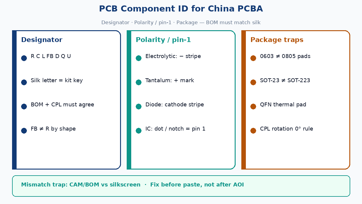
| Designator | Silkscreen letter (R, C, U…) is the assembly key — must match BOM and CPL |
| Polarity killers | Electrolytic/tantalum caps, diodes/LEDs, ICs (pin 1), polarized connectors |
| China-fab trap | CAM/BOM vs silkscreen mismatch + package alias (SOT-23 vs SOT-223) → wrong pick / wrong rotation |
| Buyer rule | Incomplete CPL/BOM = plant defaults; polarity and pin-1 notes are not optional garnish |
Procurement tip: Treat silkscreen, BOM, CPL (centroid), and assembly drawing as one controlled set. If any two disagree on refdes, polarity mark, or package, stop the traveler before paste — do not “resolve on the line.”
💡 Factory gain: China CAM catches BOM↔silk mismatches early when you ship a consistent set. Silent “similar package” substitutions are how wrong parts land under the correct designator.
Active vs passive (and why the plant cares)
| Class | Needs power to function? | Typical jobs | PCB ID cue |
|---|---|---|---|
| Passive | No | Limit, store, filter, couple | R, C, L, FB, often unmarked bodies |
| Active | Yes (bias / supply) | Amplify, switch, regulate, compute | U/IC, Q, regulators — pin-1 critical |
Passives dominate pick volume and still cause polarity failures (polarized caps). Actives dominate orientation and pin-map failures. AOI programs treat them differently: polarity libraries for diodes/caps; pin-1 / rotation for ICs and Q packages.
Through-hole (THT) vs surface mount (SMD)
| THT / DIP | SMD / SMT | |
|---|---|---|
| Mount | Leads through plated holes | Pads / lands on surface |
| Strength | Mechanical (connectors, large caps, transformers) | Density, automation, RF/small passives |
| Process | Insert → wave / selective / hand | Paste → place → reflow |
| ID habit | Body size + lead spacing + silk | Package code (0603, SOT-23, QFN…) + silk |
Mixed technology is normal. Inspection must cover both lanes: AOI polarity on SMT; THT lead protrusion, solder fill, and polarized can orientation on wave/selective. Do not assume SMT AOI covers post-wave THT polarity.
Common reference designators
| Designator | Component | Assembly note |
|---|---|---|
| R | Resistor | Includes 0Ω jumpers — not “missing parts” |
| C | Capacitor | Polarized vs non-polar: stripe / “+” rules differ |
| L | Inductor | Current / DCR matter; not interchangeable with FB |
| FB | Ferrite bead | Looks like a chip resistor/inductor — designator decides kit |
| D | Diode | Stripe = cathode (K) unless drawing says otherwise |
| LED | LED | Flat / short lead / notch = cathode; always current-limit |
| Q | Transistor / FET | Pin order from MPN datasheet — never assume |
| U / IC | Integrated circuit | Dot / notch / chamfer = pin 1 |
| Y / XTAL | Crystal / oscillator | Load-C for crystals; XO ≠ TCXO |
| J / P | Connector / header | Keying and pin-1 silk prevent reverse mate |
| SW | Switch | Debounce / mechanical life on drawing |
| F | Fuse | Fast vs slow-blow; hold current |
| T | Transformer | Isolation / pin map from datasheet |
| K | Relay | Coil polarity + flyback diode ownership |
| TP | Test point | Probe access — not a part to “stuff” unless BOM says |
| JP | Jumper | Default position on silk + assembly note |
Failure path: designator on silk says FB1, BOM line says R with a bead MPN (or the reverse). Pick feeder follows BOM package; AOI expects bead library → false fail or wrong function. Lock letter + MPN + package together.
Part families you will actually meet (short list)
Use this as a shop-floor cheat sheet, not a catalog dump.
| Family | What it does | How you spot it | Top gotcha |
|---|---|---|---|
| Resistors (R) | Limit / divide / pull | Chip brick or axial bands; 0Ω = jumper | Reading color bands wrong; treating 0Ω as open |
| Ceramic C | Bypass / decouple | Beige/black chip near IC power pins | Wrong dielectric / voltage; no polarity |
| Electrolytic C | Bulk energy | Can + negative stripe | Reverse polarity → heat / vent |
| Tantalum C | Bulk / density | Body with “+” mark | Reverse = short risk; voltage derate |
| Inductor (L) | Energy / filter | Cube, wire-wound, toroid | Confusing with FB; saturation current |
| Ferrite bead (FB) | HF noise damp | Looks like chip R/L | Kit as resistor by shape alone |
| Diode (D) | Steer / clamp / protect | Stripe = cathode | Backward = no protection or dead rail |
| LED | Indicator | Flat edge / cathode mark | No series R → instant kill |
| MOSFET / BJT (Q) | Switch / amplify | SOT-23 / SOT-223 / TO-220 / DFN | Source/drain swap; pin map |
| IC (U) | Logic / PMIC / MCU… | SOIC, TSSOP, QFN, BGA | 90°/180° rotation; QFN thermal pad void |
| Crystal / XO (Y) | Timing | Metal can or ceramic; MHz mark | Wrong load-C; XO vs crystal load |
| Connector (J/P) | I/O / power | Keyed shells, headers | Reverse insert; current rating |
| Fuse (F) | Overcurrent | Marked F; SMD or cartridge | Slow vs fast; wrong hold |
| Relay (K) | Isolated switch | Boxy; pin diagram on top | Missing coil diode; contact vs load type |
Longer specialty groups (sensors, antennas, modules, displays) follow the same rule: designator + MPN + footprint + orientation note, then placement keepouts on the drawing.
How to identify on a live board
1) Silkscreen and refdes first
Read the letter next to the part before guessing by color. Silk is the human key; CPL is the machine key. If silk is missing or crowded, the assembly drawing and BOM refdes column carry the load — say so on the RFQ.
2) Polarity and pin-1
| Part | Mark to trust | Wrong install symptom |
|---|---|---|
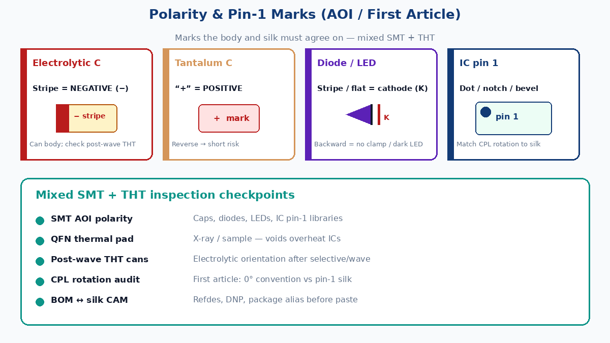
| Electrolytic | Stripe = negative | Heat, bulge, rail collapse |
| Tantalum | “+” = positive | Short / fire risk |
| Diode / many LEDs | Stripe / flat = cathode | No light; no clamp |
| IC | Dot / notch / bevel = pin 1 | Dead board; shorts on power |
| Q packages | Datasheet pin map + silk | FET body diode wrong way |
| Polarized connector | Key + pin-1 silk | Reverse power / signal |
Do not invent marks. If silk and body disagree, escalate — that is a CAM discrepancy, not a skill issue.
3) Packages (names that cause wrong picks)
| Look-alike trap | Why it hurts |
|---|---|
| 0603 vs 0805 | Pad / feeder mismatch; tombstone risk if forced |
| SOT-23 vs SOT-89 vs SOT-223 | Different pads and pinouts; “same triangle package” is false |
| Chip R vs FB vs PTC (F) | Same black brick look; designator + MPN decide |
| QFN vs QFP | Leadless vs leaded; thermal pad solder volume differs |
| SOIC rotated 180° | Pin 1 on wrong end — classic AOI / power-up fail |
4) Circuit context when docs are thin
- Caps clustered at IC VCC pins → decoupling
- Resistors on GPIO / bus lines → pull-up / down
- L + C at power entry → filter / regulator front end
- Bead on a power rail → HF suppression, not bulk energy storage
Context is a hint, not a substitute for BOM.
Selection and substitution (RFQ rules)
When stock is short, substitution is a controlled change — not a similar-looking reel.
| Must match | Why |
|---|---|
| Footprint / land pattern | Pad size, pitch, thermal pad — feeder and stencil assume it |
| Pin-1 / polarity | Same orientation language on silk and body |
| Electrical function class | TVS ≠ rectifier; FB ≠ power inductor |
| Ratings with derating | Caps ≥ ~1.5× working voltage (policy on drawing); FET Vds/Id/Rds(on); fuse hold/I²t |
| Frequency / timing behavior | Crystal load-C; bead Z vs frequency; op-amp GBW if in critical path |
| Approved AVL / MPN status | No silent EOL or broker-only swap without buyer sign-off |
Write substitution rules on the RFQ: “Footprint identical; pin-1 compatible; polarity mark orientation unchanged; electrical ratings meet or exceed BOM with stated derating; no package alias without ECO.” Plants that kit to “close enough SOT” create intermittent field fails that look like process quality.
Mixed SMT + THT inspection checkpoints
| Checkpoint | What to verify | Typical escape if skipped |
|---|---|---|
| Pre-paste BOM↔silk | Refdes, DNP, polarity marks agree | Wrong polarity program / wrong feeder |
| SMT AOI polarity | Caps, diodes, LEDs, IC pin-1 | Reverse parts pass visual “solder looks fine” |
| QFN / bottom-term | Thermal pad solder (X-ray / sample) | Overheat, early IC death |
| Fine-pitch bridges | QFP / dense SOIC | Shorts after ship |
| Post-THT polarity | Electrolytic cans, diode orientation after wave/selective | SMT AOI never saw them |
| Connector keying | Pin-1 vs mate | Field reverse-power |
| CPL rotation field | Degrees match silk pin-1 | Systematic 90°/180° on whole lot |
Testing/factory gain: AOI polarity libraries and QFN pad checks belong on the traveler for mixed builds. Wave after reflow does not inherit SMT polarity coverage for THT cans.
CAM / BOM vs silkscreen mismatch traps (China fab)
These are the traps experienced China plants flag when files are complete:
- Refdes collision — same designator on silk for two footprints, or BOM line missing from silk
- Polarity mark flipped — silk bar on anode side vs body standard
- Package alias — BOM “SOT-23” but land is SOT-223
- DNP still in CPL — machine places a “do not populate”
- Alternate MPN different pin map — same function, different pin-1
- Centroid rotation off by 90°/180° — whole reel class wrong
- Unit mismatch — μF vs nF in BOM description vs value column
Ship Gerbers + BOM + CPL + assembly drawing with one revision letter. Ask CAM for a written discrepancy list before paste. That is cheaper than sorting reverse electrolytics after AOI.
What to put in CPL / BOM for clear China assembly
BOM columns (minimum):
- Reference designator(s)
- Quantity
- MPN + manufacturer
- Description / value / tolerance (where needed)
- Package / footprint name matching CAD
- DNP flag
- Polarized Y/N + polarity note
- Approved alternates (with pin-map compatible Y/N)
CPL / centroid (minimum):
- Refdes
- X / Y (state origin and units)
- Rotation (state zero-degree convention vs pin-1)
- Side (top/bottom)
- Optional: package name echo for CAM cross-check
Assembly drawing callouts: pin-1 marks, polarized caps/diodes, THT-only designators, keepouts, torque/connector notes, and “no substitute without ECO.”
Incomplete CPL rotation notes produce beautiful solder joints on 180°-dead ICs. Complete notes are short and sit next to the BOM revision.
Common mistakes (shop-floor)
| Mistake | Prevention |
|---|---|
| Reverse electrolytic / tantalum | Stripe / “+” training + AOI polarity + THT post-wave check |
| IC rotated | Pin-1 silk vs body; CPL rotation audit on first article |
| FB stuffed as R (or reverse) | Designator-driven kitting; never kit by color alone |
| SOT family mix-up | Footprint name on BOM = CAD land; no visual alias |
| QFN cold thermal pad | Paste volume / stencil + X-ray sample plan |
| Power-up with rail short | Diode-mode / continuity on power before first bias |
| “Close enough” substitute | Written RFQ substitution rules + ECO |
Closing
Identifying PCB components well means locking designator, package, polarity, and pin-1 to the same revision of BOM, silk, and CPL. Active vs passive and THT vs SMD tell you which process and which inspection lane own the risk. China PCBA wins when CAM catches BOM↔silk traps before paste, substitution follows footprint/pin-1/polarity/derating rules, and mixed SMT+THT builds carry AOI polarity plus QFN thermal-pad and post-wave THT checks. Put those fields in the RFQ once — then the plant stops guessing under the correct silkscreen letter.