
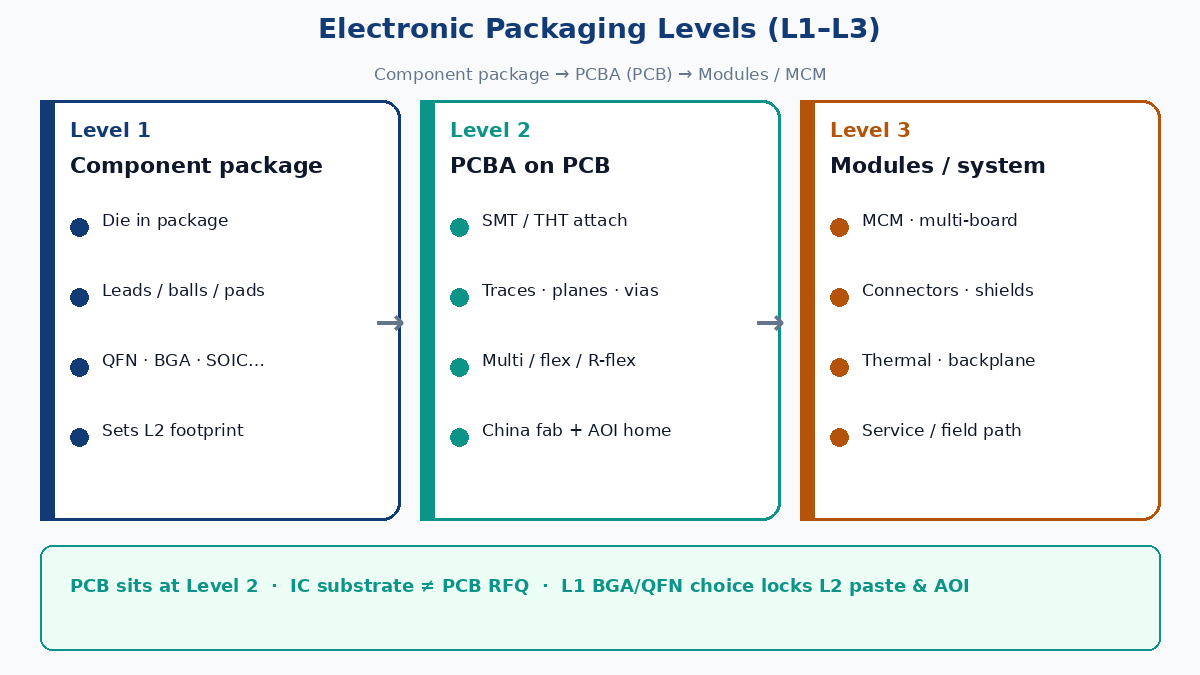
Electronic packaging levels are the hierarchy from a single packaged die to a finished module. For buyers and China fabs the useful map is Level 1 (component package) → Level 2 (PCBA on a PCB or board-level substrate) → Level 3 (modules, MCM, multi-board systems). The PCB sits at Level 2. Confusing an IC-substrate RFQ with a PCB RFQ, or picking a Level 1 BGA/QFN without Level 2 paste/AOI rules, is how quotes and yield both go sideways.
Answer first: levels, PCB seat, RFQ boundary
| Question | Factory / procurement answer |
|---|---|
| What are packaging levels? | L1 = single-device package; L2 = components on a PCB/PCBA; L3 = modules / MCM / multi-board systems |
| Where does the PCB sit? | Level 2 — the carrier that interconnects Level 1 packages into a working board |
| What is MCM? | Multi-Chip Module: several ICs (sometimes bare die) on one module substrate, treated as one functional block at Level 3 |
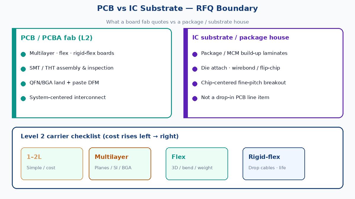
| PCB vs IC substrate? | PCB = system-centered Level 2 platform. IC substrate = chip-centered high-density transition inside a package/module — different fab, pitch, and RFQ |
| Who quotes what? | XFPCB-type fab: multilayer / flex / rigid-flex PCBs and PCBA. Package house / substrate fab: IC substrates, build-up, fine-pitch package laminates |
| Hidden yield killer | Level 1 package choice (BGA / QFN / fine-pitch) sets Level 2 footprint, paste, AOI, and X-ray constraints the China line must meet |
Procurement tip: If the drawing says “substrate” but the pitch, stackup, and panelization look like a board-level PCB, ask which plant will run it before you compare unit price. Substrate quotes and PCB quotes are not interchangeable line items.
💡 Factory gain: Lock Level 1 package → Level 2 land pattern + paste aperture + AOI/X-ray plan in one DFM pass. Changing BGA pitch after stencil release is a traveler restart, not a “minor ECO.”
Factors that drive packaging choices (all levels)
Engineers rarely optimize one metric. The same short list shows up from die attach to chassis:
| Factor | What it really means on the floor |
|---|---|
| Reliability | Lifetime vs moisture, thermal cycle, shock/vibe — maps to package type, coating, and Level 3 enclosure |
| Size / volume | Z-height, pitch, board outline — drives HDI, fine-pitch L1, flex/rigid-flex at L2 |
| Cost | Materials + assembly yield + test + rework access — cheap package, expensive paste scrap is still expensive |
| SI / PI / EMI | Controlled impedance, planes, return paths, shielding — mostly L2 stackup + L3 shields/cables |
| DFM / manufacturability | Process maturity, stencil, AOI libraries, supplier capability — China CAM will reject dream footprints |
| Repairability | Access for rework, inspection windows, connectorized L3 vs sealed MCM |
| Environment | Temp, humidity, chemicals, altitude — decide hermetic vs plastic L1, conformal coat, and module sealing |
A compact goal statement that still holds at every level: electrical interconnect + thermal path + mechanical / environmental protection. There is no universal “best” package — only what matches product, supply chain, and yield targets.
Level 1 — component packages (die becomes a part)
Level 1 packaging houses one device (especially an IC) so the die can be handled, soldered, and connected upward. Typical forms: molded plastic packages, cavity packages (hermetic or not), PGA, and the familiar SMT families (SOIC, QFP, QFN, BGA, WLCSP, etc.).
Core jobs of Level 1:
- Protect the die from moisture, contamination, and handling damage
- Present a standardized external interface (leads, balls, lands, pins)
- Carry part of the thermal path and mechanical support
Why so many styles: I/O count, pitch, thermal resistance, mechanical robustness, and cost pull in different directions. For China PCBA, the Level 1 choice is not abstract — it becomes a land pattern, paste volume, and inspection method.
| L1 package family | L2 footprint / paste sensitivity | China fab enforcement |
|---|---|---|
| Chip passives (0402–1206) | Tombstone / skew if pad imbalance | Paste aperture + pad symmetry in DFM |
| SOIC / QFP | Lead coplanarity, bridging on fine pitch | AOI lead bridging libraries |
| QFN / DFN | Thermal pad voiding, solder wicking | Paste on center pad %, X-ray sample |
| BGA | Ball pitch, void criteria, warpage | X-ray / AXI plan; keepout and via-in-pad rules |
| Fine-pitch CSP / WLCSP | Ultra-tight paste and placement | Often needs advanced SMT line + review |
Failure path: Marketing picks a 0.4 mm BGA for size; layout copies a generic footprint; stencil is standard; AOI has no ball library. First articles pass visual; field units fail under thermal cycle. Level 1 chose the pain; Level 2 paid for it.
Level 2 — PCBA (where the PCB lives)
Level 2 is assembly of Level 1 packages onto a PCB (or board-level substrate) to form a working circuit — production language: PCBA. It includes SMT / THT / mixed attach, board interconnect (traces, planes, vias), and basic thermal/mechanical design (copper pours, mounting holes, TIM pads where needed).
Common Level 2 carriers:
| Carrier | When it earns its keep | Cost structure (qualitative) |
|---|---|---|
| 1–2 layer PCB | Simple, low density, cost-first | Lowest fab; limited SI / routing |
| Multilayer PCB | Planes, impedance, dense BGA fan-out | Layer count + HDI + material drive unit cost |
| Flex (FPC) | Dynamic bend, tight 3D, weight | Polyimide + coverlay + handling yield |
| Rigid-flex | Drop connectors/cables; reliability in motion | Highest L2 fab complexity; saves L3 interconnect failures |
For most products, Level 2 is where performance, cost, and yield collide. China fab DFM at this level enforces: solder-mask defined vs non-SMD pads, paste apertures for QFN centers, BGA via-in-pad fill/cap, keepouts for AOI cameras, and panelization that survives reflow warpage.
Decision checklist — multilayer / flex / rigid-flex at L2
Use this as a buyer/engineering gate, not a catalog pitch:
- Need dedicated power/ground planes or controlled impedance? → Multilayer (often 4+).
- BGA fan-out or fine-pitch density beyond 2-layer routing? → Multilayer and/or HDI.
- Must fold into a 3D envelope or survive repeated flex? → Flex or rigid-flex.
- Connectors/cables are the dominant field failure? → Rigid-flex often cheaper in life-cycle than “cheap rigid + cable.”
- Prototype budget vs volume? → Rigid multilayer prototypes first; flex/rigid-flex when the mechanical envelope is frozen.
- RFQ clarity: Separate fab (bare board) from PCBA (stuffing). Do not bury Level 1 package assumptions inside a bare-board quote.
Level 3 — modules, MCM, and the system
Level 3 is everything beyond a single PCBA: stacking boards, connectors, harnesses, shields, heat sinks, chassis, and multi-chip modules into a subsystem or product.
Typical Level 3 forms:
- Multi-Chip Modules (MCM) — several ICs on one module substrate, often appearing externally like a large “component”
- Modular cards, mezzanine stacks, backplanes, enclosed assemblies
Why MCM shows up in Level 3 talk: It integrates heterogeneous dies, can beat a single huge monolithic die on yield, and pushes interconnect density onto a module substrate that may be laminated, ceramic, or thin-film — not the same as a commodity FR-4 PCB RFQ.
L2 → L3 handoff (failure / service path)
| Handoff item | What breaks if ignored | Service implication |
|---|---|---|
| Board-to-board connectors | Misalignment, pin damage, intermittent contact | Field swap of one board vs whole module |
| Shields / cans | EMI fail, ground loop, rework blocked | Removable vs soldered shield policy |
| Thermal (sinks, TIM, airflow) | Hot spots, derating, early L1 package death | Access for TIM rework; sensor placement |
| Backplane / midplane | Slot integrity, power distribution, SI | Hot-swap / keyed slots; cable vs board edge |
| Harness / flex tails | Strain relief, flex life, chafing | Strain-relief drawings in the traveler |
Think of Level 3 as: how boards become a serviceable, thermally and EMI-safe product in the real world.
PCB vs IC substrate — RFQ boundary (procurement)
Buyers often paste a package-substrate stackup into a PCB RFQ form. That wastes cycles.
| PCB (Level 2 platform) | IC substrate (package / MCM) | |
|---|---|---|
| Centered on | System / many components | Chip / package I/O breakout |
| Typical pitch / feature | Board-level (down to HDI microvia) | Finer build-up, often tighter L/S |
| Who quotes | PCB fab + PCBA house (XFPCB-type) | Package / substrate specialist |
| Panel / process | Standard PCB panelization, SMT | Package panel, often different materials |
| Maps to | Level 2 PCBA | Inside Level 1 or MCM Level 3 |
Mental model: An IC substrate is a high-density “mini board” inside the package story. A PCB is the primary electrical platform for the product. Substrates can sit near Level 1 or inside Level 3 MCM; they are not automatic substitutes for a PCB line item.
Reliability environment → packaging level choices
| Environment stress | Level 1 lean | Level 2 lean | Level 3 lean |
|---|---|---|---|
| High humidity / outdoor | Moisture-sensitive handling, underfill where needed | Conformal coat, sealed connectors | Gasketed enclosure, dessicant policy |
| Wide thermal cycle | Package CTE / underfill; avoid fragile CSP without analysis | Material Tg / CTE stackup; QFN void control | TIM + mechanical compliance; avoid rigid cable strain |
| Shock / vibe | Robust leaded or underfilled BGA where justified | Mounting holes, stiffeners, adhesive for tall parts | Connectors with locks; harness strain relief |
| High speed / EMI | Package parasitics matter | Impedance, planes, return vias | Shields, cable filter, backplane SI rules |
| Service / field replace | Prefer reworkable packages | Clear AOI/X-ray and rework windows | Connectorized modules over sealed MCM when service dominates |
Map the environment before freezing Level 1 packages. A plastic QFN that is fine in a climate-controlled appliance can be the wrong Level 1 choice for under-hood thermal cycle — and no amount of Level 2 paste tweak will fix the physics.
What China fab / XFPCB-type plants actually own
| Scope | In RFQ to PCB/PCBA fab | Send elsewhere |
|---|---|---|
| Bare multilayer / flex / rigid-flex PCB | Yes | — |
| SMT / THT PCBA, AOI, X-ray plan | Yes (PCBA lane) | — |
| QFN/BGA DFM (paste, VIP, keepouts) | Yes — Level 1→2 constraints | — |
| IC package substrate / build-up | No (wrong plant) | Package / substrate house |
| Die attach / wirebond / mold | No | OSAT / package house |
| Full chassis + harness build | Partial (modules by agreement) | System integrator / EMS mech |
Ship Gerber + stackup + BOM + CPL + assembly notes that name the Level 1 packages (especially BGA/QFN). Ask for a written DFM list covering paste, AOI, and X-ray before stencil cut.
Short wrap
Level 1 packages the die. Level 2 assembles packages on a PCB — that is where XFPCB-type fabrication and PCBA live. Level 3 turns boards into modules and products, including MCM. Keep substrate RFQs off the PCB quote sheet, and treat every Level 1 BGA/QFN decision as a Level 2 yield decision with paste, AOI, and environment attached.