
An electro-optic modulator (EOM) turns an electrical drive into a controlled change in optical phase, intensity, or polarization — usually through the Pockels effect. Photonics teams do not lose sleep over the crystal name on the datasheet. They lose sleep when the RF channel reflects, a via stub rings on the VNA, the stackup material eats the loss budget, or HV creepage fails before the optic ever lights. This factory note explains how an EOM works electrically, how bulk capacitive loads differ from traveling-wave loads, and what China fab notes must lock for controlled-impedance + low-loss + HV DFM driver PCBs.
Answer first: what the driver PCB must get right
| Question | Factory answer |
|---|---|
| What is an EOM? | Device that uses voltage/field on an electro-optic material to modulate light (phase / intensity / polarization) |
| Core physics | Pockels effect — refractive index ≈ linear with applied E-field |
| Bridge to electronics | Half-wave voltage Vπ sets the swing the driver must deliver |
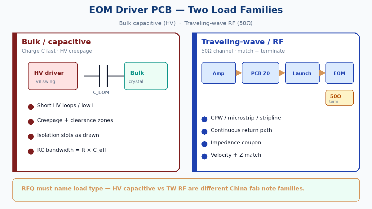
| Two electrical loads | Bulk / capacitive (charge C fast, often HV) vs traveling-wave / RF (50Ω channel, match + terminate) |
| What kills first-pass | Reflections, via stubs, wrong stackup/Dk, return-path breaks, HV spacing fails — usually visible on VNA/eye before optics |
| China fab must lock | Target Z0, stackup/Dk note, loss budget, finish, impedance coupon, HV creepage class |
Buyer rule: an RFQ that only says "EOM driver PCB, 50Ω, high voltage" without load type, stackup note, coupon, and creepage class will get non-comparable quotes and CAM defaults that favor panel yield over your RF/HV intent.
💡 Procurement tip: Put bulk capacitive vs TW on the traveler as different fab note families — HV isolation vs RF CPW/microstrip/stripline. Do not let one generic "RF board" note cover both.
How an EOM works (electrical view)
Applied voltage on the electrodes creates an electric field in the electro-optic material. The refractive index shifts (Pockels). Optical phase shifts. That phase change is used directly, or converted into intensity or polarization change downstream.
Chain: Voltage → Field → Index → Phase → (optional) Intensity / Polarization
Drive waveform distortion therefore shows up optically. The PCB and driver do not rewrite the crystal physics — they decide whether the field at the electrodes matches the intended waveform.
Half-wave voltage Vπ
Vπ is the voltage that produces a π radian phase shift under the stated optical and electrode geometry. It depends on material, interaction length, electrode spacing, wavelength, and device layout. Lower Vπ eases voltage swing; it does not erase capacitance, bandwidth, or matching problems. Quote drivers on voltage + capacitance (or Z0) + frequency / edge rate, not voltage alone.
Phase, intensity, polarization
| Mode | What changes | Typical electrical note |
|---|---|---|
| Phase | Optical phase; power ideally steady | Clean drive waveform; bias stability if used |
| Intensity | Power (e.g. Mach–Zehnder interferometric path) | Bandwidth + bias point care |
| Polarization | Polarization / birefringence control | Same field-drive rules; optical analyzer side separate |
Bulk vs waveguide — different fab notes
| Feature | Bulk EOM | Waveguide / integrated EOM |
|---|---|---|
| Optical path | Free-space crystal | Guided waveguide |
| Typical electrical worry | Higher voltage, capacitance | Higher RF bandwidth, matching |
| Electrical model | Often capacitive | Often distributed / traveling-wave |
| Common use | Laser systems, Q-switch style | Telecom / high-speed photonics |
| Main PCB challenge | HV creepage/clearance, low inductance switching | 50Ω RF channel, vias, stackup, termination |
| Fab note family | HV spacing, copper weight, isolation slots | Controlled Z0, CPW/microstrip/stripline, coupon, low-loss material call |
Treat these as different jobs on the PO. A bulk capacitive driver that is fabbed like a microwave TW board (or the reverse) is how teams burn a rev on the wrong DFM checklist.
Specs that matter to the driver and the fab
| Parameter | Meaning | Driver / PCB relevance |
|---|---|---|
| Vπ | Voltage for π phase shift | Driver swing |
| Bandwidth | Useful modulation band | RF bandwidth / edge rate |
| Insertion loss | Optical through loss | Link budget (optics); not a copper thickness substitute |
| Extinction ratio | High vs low optical contrast | Modulation quality target |
| Input capacitance | Lumped electrical load | Rise time, driver current, RC limit |
| RF impedance | High-frequency port Z | Matching, reflections, termination |
Electronics-facing RFQs should prioritize Vπ, C or Z0, bandwidth, termination, HV class. Optical-only fields without electrical load type do not guide CAM.
Capacitive load vs traveling-wave load
Capacitive / lumped: driver must charge the EOM (+ pad + via + connector parasitics) fast enough. Rough RC view: τ ≈ R × C_eff. Extra copper, fat pads, and stubby launches raise C_eff and steal bandwidth before the crystal is to blame.
Traveling-wave: RF propagates along electrodes with the optical wave. Design cares about velocity match (RF vs optical) and impedance match (reflections). Termination and continuous reference matter as much as amplifier watts.
| Capacitive / bulk-style | Traveling-wave | |
|---|---|---|
| Success metric | Charge fast, survive HV | Deliver clean RF to electrode + terminate |
| PCB geometry | Short HV loops, low L, isolation | Continuous Z0 line (microstrip / CPW / stripline) |
| Fab emphasis | Creepage/clearance, HV DFM | Impedance control, coupon, material/loss |
| Failure tells | Arcing, overshoot, slow edges | Bad S11, eye collapse, stub resonance |
Driver types: broadband, resonant, TW
- Broadband — wide frequency or arbitrary waveforms. Needs bandwidth, Z control, low parasitics, reflection control.
- Resonant — LC boost near a fixed frequency. Voltage gain for a narrow band; wrong for "variable RF" RFQs.
- Traveling-wave oriented — treat channel as transmission line end-to-end: amp → PCB → connector/cable → EOM → termination.
Name the driver class on the RFQ so the plant does not invent a resonant layout for a broadband TW load.
RF channel as one 50Ω structure
A typical high-speed path:
RF amp → PCB trace → connector launch → cable/module → EOM → termination
A "50Ω trace" on one layer does not make a 50Ω channel. Connectors, vias, layer hops, and the EOM interface all contribute discontinuities. Design and fab notes should treat the trace + return path as one electromagnetic structure, with target Z0 stated (usually 50Ω single-ended unless the drawing says otherwise).
Stackup, vias, return path
Stackup and geometry must be defined together: trace width/gap, copper weight, dielectric thickness, Dk callout, reference plane. Microstrip, stripline, or CPW — pick from frequency, shielding, and length, then lock in fab notes.
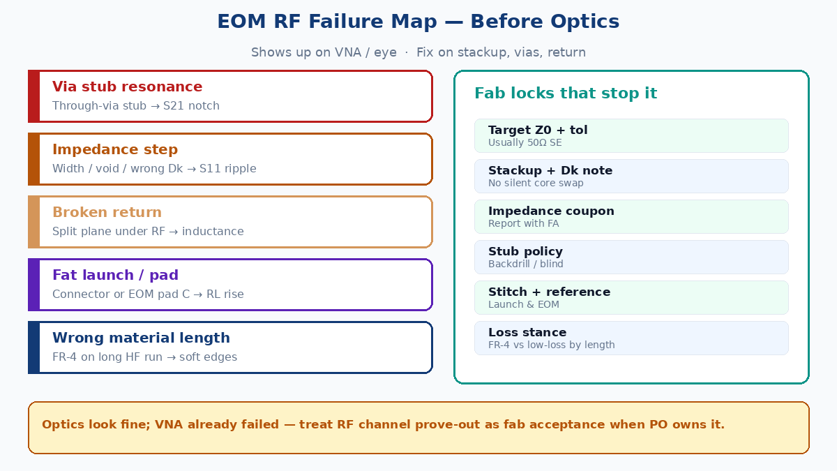
Via / stub / return failure map (shows on VNA/eye before optics):
| Failure | Electrical symptom | Typical cause |
|---|---|---|
| Impedance step | Reflection / ripple in S11 | Width change, unfinished plane void, wrong Dk assumption |
| Long via stub | Resonance notch | Through-via to thin signal layer without backdrill / blind |
| Broken return | Extra inductance, EMI | Split plane under RF, missing stitching near launch |
| Fat pad / connector launch | Return loss rise | Untuned launch, oversized anti-pad |
| Excess C near capacitive EOM | Slower edges | Huge pads, unused copper islands |
| Wrong material for long HF run | Loss / soft edges | FR-4 on a long GHz channel without loss budget review |
Factory language that sticks:
- "Target Z0 = 50Ω (state tolerance); impedance coupon required."
- "Stackup with Dk note for RF layers; do not substitute core/prepreg without written approval."
- "Minimize RF layer changes; backdrill or blind vias where stub length threatens band."
- "Continuous reference under RF; stitch near connector and EOM launch."
Material choice (qualitative — no invented Df)
| Situation | Qualitative material stance | Cost / process note |
|---|---|---|
| Short run, modest frequency, capacitive HV driver | Standard FR-4 / high-Tg FR-4 often enough if HV spacing and inductance dominate | Lowest cost; still call HV class |
| Longer channel, higher frequency, TW / broadband | Prefer low-loss laminate on RF layers (or hybrid RF+FR-4) | Higher material $; need stackup approval and coupon |
| Mixed bias + RF + HV on one board | Segment: RF on controlled stack; HV on isolation rules; bias away from heat | Hybrid stack / zone layout DFM |
Do not invent dissipation-factor numbers on the RFQ. State frequency band, channel length intent, and loss budget qualitatively ("low-loss RF laminate required above X for length Y — plant propose stackup"). Let CAM and the laminate house close Dk/Df with the coupon plan.
High-voltage creepage and clearance
Bulk drivers can sit at hundreds to thousands of volts. PCB must provide:
- Clearance — shortest air path between conductors
- Creepage — shortest path along the surface
Spacing depends on working voltage, transients, pollution degree, and the equipment safety drawing — not on a slogan. Fast edges also need low loop inductance to limit overshoot into adjacent nets.
HV fab notes: isolation slots as drawn, no copper/silk across barriers, creepage class or mm zones from the insulation diagram, copper weight if current/thermal demands it. "HV safe" with no zone map is not a quote input.
Bias vs RF — segregate and manage heat
Interferometric intensity modulators often need a stable bias point. Temperature and coupling from RF power stages shift that point and move the optical operating point.
| RF path | Bias / control path |
|---|---|
| Bandwidth, Z0, RF loss | Low noise, precision |
| Return continuity | Drift / thermal stability |
| Power amp heat | Keep sensors and bias DACs off hot copper |
Factory layout DFM: segregate RF and bias zones; keep thermal copper / pours from cooking the bias feedback; separate return strategies where the schematic requires it. Automatic bias (optical tap → photodetector → controller → bias) needs clean analog layout, not an RF afterthought.
Common PCB problems → EOM impact
| PCB problem | Electrical effect | Possible EOM impact |
|---|---|---|
| Impedance discontinuity | RF reflection | Distorted drive / poor extinction |
| Excess parasitic C | Bandwidth loss | Slower modulation |
| Long via stub | Resonance | Band notches on VNA |
| Poor return path | Inductance / EMI | Unstable drive |
| Weak connector launch | Return loss | Reduced usable band |
| Insufficient HV spacing | Leakage / arc | Reliability fail |
| Thermal coupling into bias | Bias drift | Unstable optical output |
PCB faults do not change the Pockels coefficient. They change the field that reaches the crystal.
Selection checklist (architecture before Gerber)
Confirm before layout and before RFQ:
- Modulation type — phase / intensity / polarization
- Wavelength and optical interface (context for Vπ conditions)
- Bandwidth or edge-rate need
- Vπ and drive swing
- Load type — capacitance vs RF Z0 + termination
- Broadband / resonant / TW driver class
- RF termination ownership
- HV isolation / creepage class if applicable
- PCB loss budget and material stance
- Bias and thermal stability needs
China fab RFQ fields for EOM driver PCBs
Copy these so procurement gets comparable quotes:
- Target Z0 (e.g. 50Ω ±tol) and single-ended vs differential
- Stackup / Dk note for RF layers; hybrid allowed Y/N; no silent substitute
- Loss budget qualitative — frequency band + channel length intent; low-loss laminate required Y/N
- Finish — ENIG / immersion Ag / etc. (state one; RF launch sensitive)
- Impedance coupon required; report format
- HV creepage class or zone map / slot callouts from insulation drawing
- Load type — bulk capacitive vs TW (drives HV vs RF CPW/microstrip fab notes)
- Via / stub policy — backdrill / blind where needed; RF layer-change limits
- Bias/RF segregation and thermal copper notes on fab drawing
- Electrical acceptance — VNA/S-parameter or TDR window if the PO owns RF prove-out (optics optional for fab FA)
Incomplete electrical notes become FR-4 defaults, missing coupons, and HV spacing that CAM shrinks for yield. Complete notes are short and sit next to the stackup PDF.
Closing
EOM performance is system-level: the crystal sets how light responds to a field; the driver PCB decides whether that field is clean, matched, and safe. For China fab work, say the load type out loud, lock Z0 + stackup/Dk + coupon + loss stance, and state HV creepage where bulk drivers need it. Segregate bias from RF heat. Fix via stubs and return breaks on the VNA before blaming the optic. That is how photonics RFQs stop being "50Ω high voltage somehow" and become a manufacturable controlled-impedance + HV DFM job.