
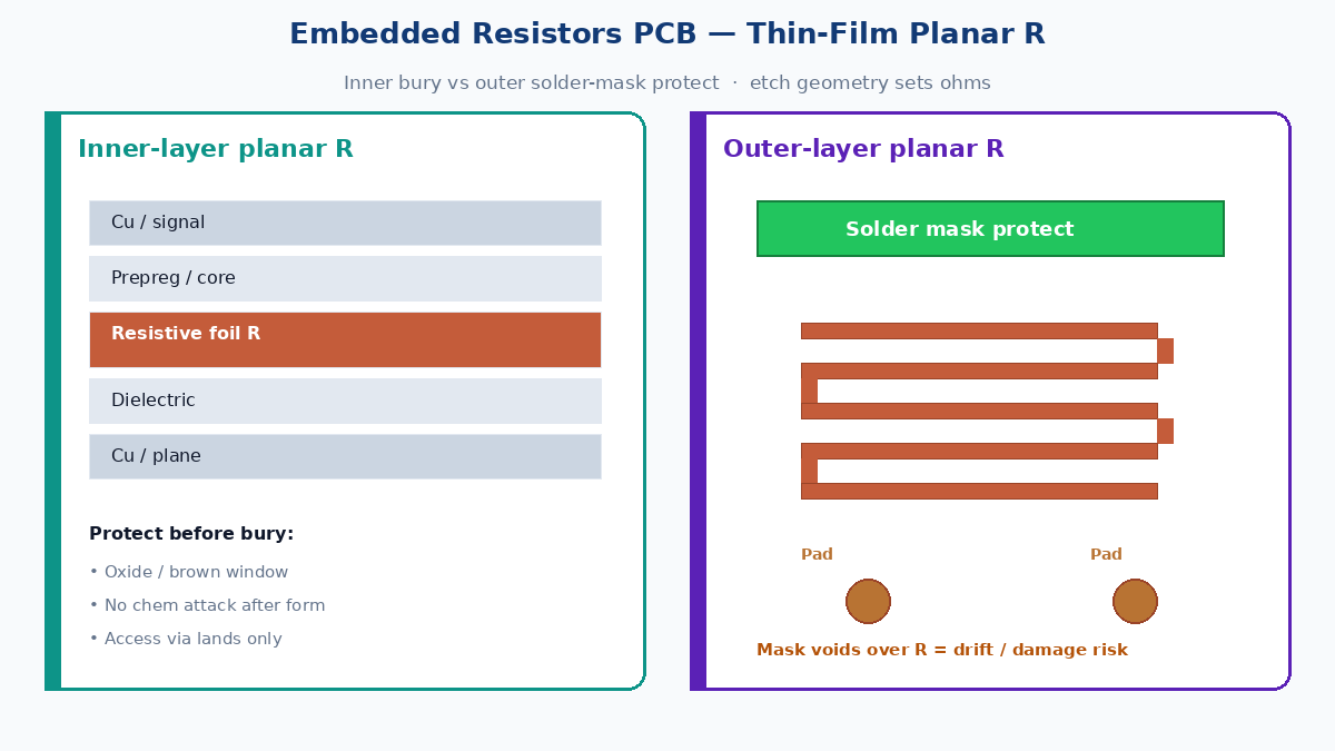
An embedded resistor is a planar resistive element formed inside or on a PCB layer — not a chip soldered on the surface. Most production builds use thin-film (formed) resistors: a resistive foil laminated to dielectric, then patterned by photolithography and selective etch so length, width, and sheet behavior set the ohms. Buyers choose them to free surface area, cut some via hops, shrink the outline, or tighten high-speed termination paths. Yield and tolerance live or die on etch geometry, outer-layer mask protection, and whether downstream chem (micro-etch, browning/oxide) is compensated in CAM or corrected by laser trim.
Answer first: what it is, how made, accuracy control
| Question | Factory / procurement answer |
|---|---|
| What is an embedded resistor? | Planar R built into the board stack (inner or outer) from resistive foil + subtractive patterning — not an SMT chip |
| How is it made? | Laminate resistive foil → photo pattern → 3 etches across an 8-step flow → strip → protect (outer: solder mask) → finish stack |
| Accuracy control? | Etch endpoint + geometry; protect exposed R from chem attack; CAM compensate expected drift; optional laser trim for tight tol |
| Why use it? | Surface space, fewer vias, smaller board, SI / termination closer to the route |
| Fear list (implicit) | R drifts after oxide / micro-etch; fab cannot hold tol without trim; RFQ silent on layer / foil / coupon |
💡 Procurement tip: Put target Ω, tolerance, laser trim Y/N, layer (inner/outer), foil system (generic), and coupon / acceptance on the RFQ. “Add embedded R” with no tol or trim flag is how quotes diverge and travelers invent defaults.
Why designs embed resistors
| Driver | What changes on the board |
|---|---|
| Surface real estate | Discrete chips leave pads, keep-outs, and placement islands; planar R frees that area for ICs, connectors, or routing |
| Via count | Some surface terminations need vias to reach inner nets; embedding near the net can drop hops |
| Outline / stack height | Moving passives into the stack can shrink XY or ease ESD / clearance crowding |
| Signal integrity | Termination or pull networks sit closer to the controlled route — less stub, less package parasitics |
Embedded R is not free density. It trades SMT reworkability and catalog flexibility for fab process control. If the BOM still needs wide Ω range, frequent ECO swaps, or field replaceability, discrete SMT often still wins.
Thin-film / planar — what CAM actually builds
In production talk, “embedded resistor” usually means a thin-film formed (planar) resistor: resistive foil laminated with dielectric, then subtractively patterned with copper.
- Can sit on inner layers (space-critical, buried after lamination) or outer layers (must be mask-protected).
- Dielectric partners commonly include FR-4, polyimide, and PTFE — same foil family can ride rigid or flex constructions when the fab qualifies the stack.
- Call the material family on the PO as a generic resistive-foil system (supplier / construction as approved). Do not treat a brand name as a process traveler substitute.
Geometry rules: resistance tracks effective length, width, and the foil’s sheet behavior after etch and chem exposure. This article does not invent sheet-resistance numbers — lock Rs and geometry rules with the foil datasheet and the fab’s process window.
Process flow — 8 steps, 3 etches
Thin-film planar R uses photolithography plus selective etching. Typical flow:
- Apply photoresist on the foil/copper stack.
- Expose and develop the copper + resistor pattern.
- First etch — remove unwanted copper; establish the copper pattern.
- Second etch — remove unwanted resistive layer (often copper-sulfate chemistry) while holding copper edge accuracy.
- Strip the first resist.
- Reapply photoresist and develop the final copper/resistor window.
- Third etch — alkaline (or fab-qualified) selective copper removal to expose the resistor body without attacking the resistive film.
- Strip again — resistor formation complete; then protect / laminate onward.
Why three etches (not one)
| Etch | Job |
|---|---|
| 1 | Clear excess copper → initial Cu pattern |
| 2 | Clear excess resistive film → keep Cu geometry honest |
| 3 | Open / define the R region → expose planar resistor without wrecking the film |
One-bath “etch everything” control is too coarse. Split chemistry is how fabs separate copper definition from resistive-film definition and from the final expose step that decides ohms.
Inner vs outer — protection is not optional
| Location | Protection | Factory note |
|---|---|---|
| Inner layer | Buried under subsequent prepreg / cores after formation | Chem attack window is mainly before final bury (oxide/brown, cleans). After bury, mechanical damage risk drops; electrical access is via lands/vias only |
| Outer layer | Solder mask over the resistor body | Mask reduces scratch and later wet-process attack. Openings must not leave R film unprotected in wash / HASL / ENIG prep unless designed that way |
Outer-layer R without a defined mask strategy is a drift and damage lottery. Inner-layer R without oxide/brown discipline is the same lottery one step earlier.
Etching precision — geometry is the ohms
Final resistance follows finished length, width, corners, and edge quality — not the CAD polyline alone. Over-etch narrows or lengthens the effective path; under-etch leaves bridges or wrong aspect. Endpoint control on etch 3 (and etch 2 edge fidelity) is the day-to-day accuracy lever before any trim.
Factory checklist:
- Etch endpoint / undercut window locked on the traveler
- Artwork compensation for known undercut (separate from chem-drift CAM below)
- Coupon geometries that match production R styles (serpentine, bar, net)
- No silent change of etchant or spray parameters mid-lot
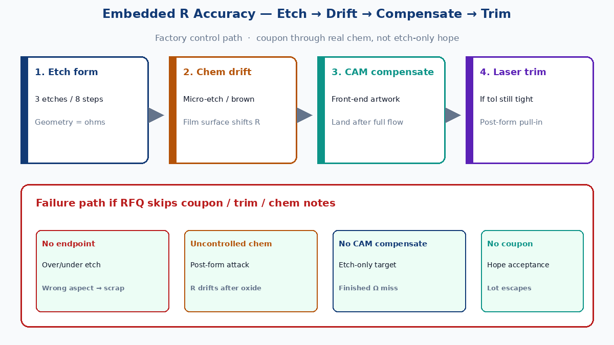
Downstream chem → R drift failure path
Resistance is not “done” when step 8 strips. Later wet steps that touch the exposed film move ohms:
| Later step | Why R can shift |
|---|---|
| Pre–solder-mask clean / micro-etch | Acid micro-etch thins or roughens the resistive surface |
| Inner-layer browning / oxide | Oxide chem meant for Cu adhesion can attack unprotected R film |
| Other acid cleans | Same surface-attack class |
Failure path (factory): etch forms R within window → oxide or micro-etch attacks film → sheet / geometry effective change → finished Ω out of tol → scrap or silent field drift if never coupon-checked.
Controls that actually work
- Tighten the chem window — pre-mask and brown/oxide recipes that bond copper without eating R film.
- Protect before attack — mask on outer; process order and covers on inner where possible.
- CAM front-end compensation — if the full flow is known to shift R by a characterized amount, CAM adjusts geometry or target so after chem the board lands near the PO value. Compensation is a design+fab strategy, not a magic etch tweak.
- Laser trim when etch + compensate still cannot hold the tolerance.
Characterize drift on coupons through the real flow, not on a dry etch-only sample.
Laser trim — when etch control is not enough
Laser trim cuts or modifies the planar resistor after formation to pull ohms into a tighter band. Use it when:
- PO tolerance is tighter than the fab’s etch + compensate capability
- Mix of R values on one panel needs post-form correction
- High-reliability acceptance requires measured-in-tol evidence, not artwork hope
Trim adds cycle time, equipment, and a scrap mode (over-trim / microcrack). Call trim Y/N and target tol on the RFQ so the quote includes the real process, not an etch-only fantasy.
Advantages vs trade-offs
Advantages
- Surface space freed for actives and connectors
- Fewer vias for some networks
- Path to smaller outline / denser packaging
- SI-friendly placement of terminations near the route
- Works across common dielectrics (FR-4, PI, PTFE) when qualified
- Applicable to rigid and some flex constructions
Trade-offs / costs
- Etch precision and three-chem control
- Downstream chem compatibility and drift risk
- CAM compensation engineering + coupon discipline
- Laser trim cost for tight tol
- Rework: you cannot swap an 0402 after the board ships — ECO means fab change or board scrap
- Yield learning curve on first articles
When discrete SMT still wins
| Situation | Prefer discrete SMT chip |
|---|---|
| Wide Ω catalog / frequent value ECOs | Chip swap beats fab artwork change |
| Loose placement density | Surface chips are cheaper and faster to quote |
| Field / depot rework required | Embedded R is not field-replaceable |
| Fab has no qualified foil + etch + trim line | Do not force embed on an unready traveler |
| Prototype speed over density | SMT proto, embed only when density/SI justifies NRE |
| Very tight tol without trim budget | Buy precision chips; or fund trim on embed |
Decision rule: embed when density, via budget, or SI placement pays for process control; keep SMT when cost, rework, yield learning, or value flexibility dominate.
Test / coupon acceptance for embedded R
Agree acceptance before build — not after panels fail:
| Check | What it proves |
|---|---|
| Layer coupon with same foil + geometry family | Etch + chem flow lands near target Ω |
| Pre- vs post-oxide / post-micro-etch coupon read | Quantifies drift for CAM compensate |
| Finished-board net measurement (where accessible) | Outer or via-accessible R meets tol |
| Laser-trim log (if used) | Pre-trim / post-trim distribution |
| Visual / AOI on outer R + mask coverage | Opens, scratches, mask voids over R |
| Microsection (sample) | Film integrity, undercut, interface |
Put coupon locations, measurement method, temperature note, and pass/fail on the PO. “IPC generic” without an R coupon plan does not protect embedded resistor lots.
China fab RFQ fields (copy into the PO)
Minimum set that stops silent defaults:
- Target Ω per resistor (or table) + tolerance
- Laser trim — Y/N; if Y, trim window and max trim cycles
- Layer — inner layer ID(s) or outer; mask protect note for outer
- Foil system — generic resistive-foil construction / approved supplier family (no brand-as-only-spec)
- Coupon — geometry, count, measure stage (post-etch / post-oxide / finished)
- CAM compensate — allow Y/N based on fab characterization
- Acceptance — measurement method, sample plan, temperature
- Stack context — dielectric family (FR-4 / PI / PTFE), finish, and any chem that will see exposed R
Incomplete notes become “etch whatever and hope.” Complete notes are short and sit next to the stack-up table.
Bottom line: Embedded resistors earn their keep when planar R frees space, vias, or SI path length that discrete chips cannot. Manufacturing success is three controlled etches, inner/outer protection, chem-drift awareness with CAM compensate, and honest trim/coupon rules on the RFQ — not a slogan about “embedded passives.” XFPCB can review foil system, layer plan, tol, and coupon acceptance with your Gerbers before the traveler locks.