
You need ESP32 PCB files that a China fab can actually build — not a mirror of vendor Gerbers, and not a board that passes DRC then fails Wi-Fi or brownout on first power-up. This factory guide shows how to start legally from official module / chip references, then package an ESP32-module (or chip-down) release zip: antenna copper-keepout, power and USB checks, footprint pin-1 traps, and a Gerber / BOM / CPL checklist China CAM opens without inventing defaults.
Answer first — what “ESP32 PCB files” means for a China RFQ
| Intent | Do this | Do not do this |
|---|---|---|
| Get files / start design | Download official hardware design guides and reference designs from the module or chip vendor; build your schematic and board | Host, mirror, or redistribute third-party Gerbers as if XFPCB (or any fab) supplies them |
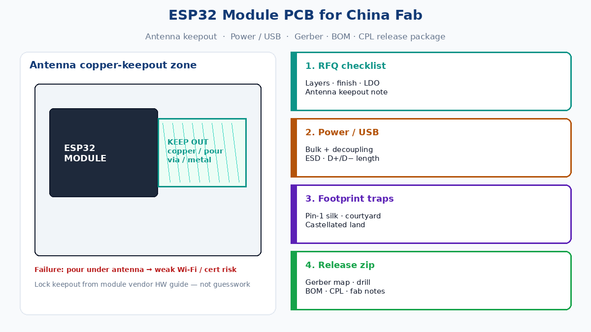
| Survive RF | Copy the vendor antenna keepout (copper, pour, via, metal, tall parts) into copper + courtyard layers | Guess keepout from a photo or pour GND under the antenna region |
| Survive power | Size 3V3 for Wi-Fi TX peaks; place bulk + local decoupling per vendor | Starved LDO / thin pour → brownout when radio transmits |
| Survive USB | ESD path, D+/D− length/match notes, connector mechanical | “USB works on the breadboard” as the only check |
| Pass China CAM | One-rev zip: Gerber map, PTH/NPTH, stack/finish/class, BOM+CPL if PCBA | Mixed revs, missing NPTH, blank finish, BOM with no MPN |
One-line definition: A fab-ready ESP32 package is your board derived from legal vendor references, with RF/power/USB gates closed and a complete Gerber/BOM/CPL zip — not a download dump of someone else’s project.
💡 Procurement tip: Put “antenna keepout per module HW guide rev X” and “3V3 rail capable of Wi-Fi TX peak” on the RFQ / fab notes. CAM cannot invent RF clearances from a blank readme.
Legal start — official references only
Espressif and module makers publish public reference designs and hardware design guidelines. Use those as the legal starting point:
- Identify the exact module MPN (or bare ESP32 package) your BOM will buy
- Open that product’s hardware design guide and land-pattern / keepout drawings from the manufacturer site
- If a public reference schematic/layout exists for that family, treat it as a study aid — re-implement under your company part numbers and stackup
- Export your Gerbers after DRC against the fab capability sheet
XFPCB fabricates and assembles from customer-owned files. We do not host, mirror, or redistribute Espressif, Adafruit, SparkFun, or other third-party Gerber packages. Asking a fab for “the ESP32 download pack” is the wrong ask — ask for DFM on your release zip.
Open-source community boards are useful for learning, but redistribute only under their license and never present them as the fab’s catalog. For production RFQ, prefer a controlled internal design with frozen MPNs.
Module vs bare chip — buyer decision
| Factor | ESP32 module on your PCB | ESP32 bare chip (chip-down) |
|---|---|---|
| RF / antenna | Module brings certified RF front-end + antenna or U.FL path; you still must honor keepout | You own RF matching, antenna, and usually a harder cert path |
| Time to first spin | Faster for most IoT / consumer / industrial gateways | Longer layout + RF bring-up |
| Board area / cost | Module costs more; board layout simpler | Cheaper at volume if you have RF skill |
| Footprint risk | Castellated / stamped land pattern + pin-1 silk traps | BGA/QFN pitch, fan-out, impedance |
| When buyers choose it | Prototypes, mid volume, teams without RF specialists | High volume, tight form factor, in-house RF |
Default for most China fab buyers: start with a module footprint + vendor keepout. Move chip-down only when volume and RF ownership justify it.
Antenna copper-keepout — the factory failure path
The failure path is boring and expensive:
- Designer pours solid GND or routes under the module antenna region
- Board passes copper DRC (rules never encoded the keepout)
- Assembly looks fine; Wi-Fi range is poor or fails radiated tests
- Respin: cut copper, move metal cans, shift connectors
Factory controls:
| Control | Why |
|---|---|
| Draw keepout on copper and courtyard / fab drawing from the module HW guide | DRC and human review both see it |
| No copper, vias, pours, or metal stiffeners in the keepout | Antenna pattern depends on clearance |
| Keep tall metal (shields, screws, batteries) out of the keepout volume | Near-field detuning |
| Note board edge / “antenna at edge” rules from the guide | Edge fire vs center mount changes radiation |
| Call keepout out in fab notes / assembly drawing | Second pair of eyes at CAM / SMT |
Do not invent millimeter keepout numbers in marketing copy. Copy the dimensions from the revision of the guide that matches your MPN.
Power — brownout when Wi-Fi transmits
ESP32 Wi-Fi TX draws sharp current peaks. Thin 3V3 pours, undersized LDOs, long inductive USB 5V paths, and missing bulk caps cause resets that look like “firmware bugs.”
Release checks:
- Regulator headroom and current rating for TX peaks, not only idle
- Bulk capacitor near the module 3V3 entry + local ceramics per vendor
- Separate analog / RF sensitive returns only as the guide requires — do not invent exotic splits that break return paths
- Inrush and USB VBUS limits if bus-powered
- Brownout detector thresholds aligned with real rail sag under TX
On the RFQ, “3V3 rail designed for Wi-Fi TX peak per module guide” beats “power OK.”
USB — ESD, D+/D−, and connector mechanics
If the board exposes USB:
- Place ESD protection where the guide / connector practice expects it
- Keep D+/D− short, matched, and away from noisy switchers when possible
- Respect connector footprint, shell grounding, and mechanical keepout
- Do not route USB under the antenna keepout or across unbroken RF ground slots without a plan
USB that “enumerates on the lab cable” can still fail ESD or radiated coupling in the field.
Module footprint — pin-1 and silk traps
Module footprints trip first articles more often than people admit:
| Trap | Symptom | Fix |
|---|---|---|
| Pin-1 ambiguity | Module rotated 180° | Silk pin-1 mark on board and assembly drawing; match vendor pin-1 |
| Castellated land undersize | Open / weak joints | Land pattern from vendor drawing, not a free library guess |
| Courtyard collision | Shield / connector hits module | 3D or paper mock of height + keepout |
| Paste / stencil | Tombstone or poor heel on castellation | Stencil aperture note for module pads |
| NPTH / mechanical holes | Mounting holes plated by mistake | Separate PTH vs NPTH in drill package |
Lock the library part to the MPN datasheet before place. Do not nudge pads only on one board revision.
China fab RFQ checklist — ESP32 module boards
Paste this into the RFQ or fab-notes PDF:
| Field | What to specify |
|---|---|
| Layers / stack | Layer count, thickness, copper weight, Tg if needed |
| Finish | ENIG / HASL / etc. — match fine-pitch and module land needs |
| Soldermask / legend | Color; pin-1 and polarity visibility |
| IPC class | Class 2 vs 3 stated, not blank |
| Antenna keepout | “Per module HW guide rev ___; no copper/via/metal in zone” |
| Module land | MPN + land pattern source; pin-1 orientation drawing |
| Power note | 3V3 capable of Wi-Fi TX peak; decoupling intent |
| USB / ESD | If used: protector MPN, connector MPN |
| LDO / PMIC | MPN on BOM; thermal copper if needed |
| Impedance | Only if chip-down RF / controlled USB HS requires it — with stack table |
| Qty / lead time / ship-to | Standard commercial fields |
| Files | See release package below |
Release package — Gerber / BOM / CPL completeness
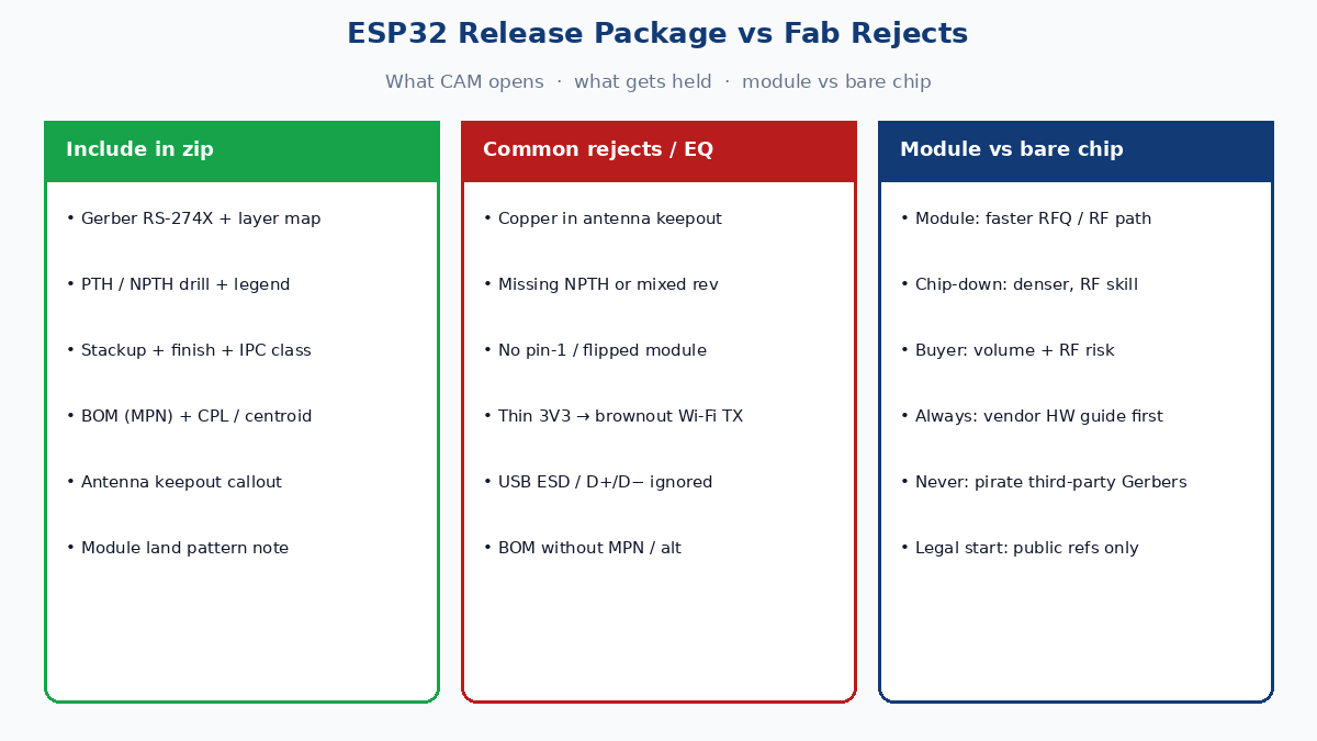
One revision letter across all files. CAM rejects mixed Gerber A / BOM B more than exotic stackups.
| File | Required content |
|---|---|
| Gerbers (RS-274X) | All copper, mask, paste, silk; filename→layer map in readme |
| Drill | Excellon PTH and NPTH separated (or clear hole chart) |
| Stackup / fab notes | Finish, thickness, class, keepout callout, special tolerances |
| BOM | MPN, refdes, qty, approved alts; module and LDO called out |
| CPL / centroid | Refdes, side, X/Y, rotation — for SMT |
| Assembly drawing | Pin-1, polarity, keepouts, no-stuff options |
| Optional | IPC-356 netlist on dense boards; 3D STEP for mechanical EQ |
Incomplete package failure path: zip missing NPTH → fab plates mounting holes → module mechanical interference or shorts → EQ hold or scrap.
CAD workflow notes (KiCad / other EDA — principles only)
Tool brand does not matter to CAM. Habits do:
- Library lock to datasheet land pattern before place
- Place module and antenna edge / keepout first; then power; then USB; then signals
- Encode keepout in rules or dedicated keepout layers so DRC fails if copper invades
- Run DRC against the quoted fab capability (trace/space, annular ring), not a hobby default
- Export the zip above; open Gerbers in a viewer before RFQ
EasyEDA / cloud tools and desktop tools all fail the same way: pretty schematic, incomplete zip, copper in keepout.
Soft next step
When your ESP32 module board zip is ready — Gerbers with layer map, drill, stack/finish/class, antenna keepout note, BOM and CPL — send it for China fab DFM and quotation. XFPCB reviews manufacturability and assembly risk on your files; we do not substitute pirated reference Gerbers for an engineering package.