
ENIG (Electroless Nickel Immersion Gold) is a two-metal PCB surface finish: an electroless nickel-phosphorus barrier on copper, capped by a thin immersion gold that keeps nickel solderable through storage and shipping. Fab notes that only say “ENIG” leave nickel/gold thickness, XRF acceptance, and black-pad bath control to the house default. This factory guide covers the Ni+Au stack, process steps, IPC-4552 thickness language, ENIG vs HASL/OSP/ImAg/ENEPIG/hard gold, selective ENIG, when to use it, and an incoming QC checklist for China quotes.
What ENIG is — and what each layer does
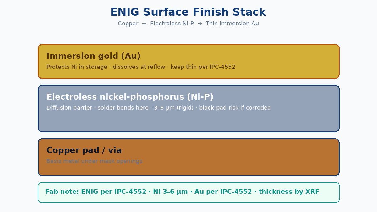
ENIG is chemical plating, not electrolytic “hard gold.” After solder mask, exposed copper pads and vias receive:
| Layer | Role | What fails if it is wrong |
|---|---|---|
| Electroless Ni-P | Diffusion barrier; the surface solder actually bonds to after gold dissolves | Thin/porous Ni → copper attack, weak IMC path; hyper-corroded Ni → black pad / non-wet |
| Immersion Au | Protects nickel from oxidation in storage; dissolves into solder during reflow | Too thin / porous → nickel oxidizes before assembly; over-aggressive Au chemistry → nickel corrosion risk |
Typical stack: Cu → electroless Ni-P → thin immersion Au. Gold is not the solderable bulk metal. During soldering the gold dissolves; the joint forms on nickel (Ni-Sn IMC family). Buying “more gold” for solder strength is the wrong lever — and thick gold is a cost and embrittlement risk, not a reliability upgrade.
💡 Procurement tip: Put thickness and metrology on the fab note, not only the word ENIG. Silent drawings invite house defaults that pass visual gold color but miss your XRF window.
Process steps (factory traveler view)
ENIG is autocatalytic / displacement chemistry — no external plating current on the board for the Ni/Au stack. A controlled line roughly does:
- Clean / micro-etch — strip oxide, organics, and leave a fresh copper topography for adhesion.
- Activation — typically a palladium catalyst so electroless nickel nucleates uniformly on copper.
- Electroless nickel — Ni ions reduce (commonly hypophosphite chemistry) into a continuous Ni-P layer. Phosphorus content and bath health drive corrosion resistance and solderability together — not as separate marketing knobs.
- Immersion gold — displacement: gold ions exchange with surface nickel until a thin Au film covers the Ni; the reaction self-limits. Aggressive gold baths or poor rinse discipline are classic black-pad contributors.
- Rinse / dry / measure — XRF thickness on defined pad features; solderability / visual gates per the quality plan.
Between steps, rinse integrity matters as much as bath recipes. Cross-contamination (nickel drag-in, gold contamination, organics) shows up later as non-wet pads that still look gold under casual light.
IPC-4552 thickness — the fab-note line that sticks
IPC-4552 is the industry performance language for ENIG thickness and related process expectations. For rigid boards, the electroless nickel window commonly cited from the specification family is 3–6 μm. Immersion gold is intentionally thin; modern IPC-4552 revisions treat gold with statistical acceptance (mean and sigma limits in the ~0.04–0.10 μm class), not “gold as thick as possible.”
Exact fab-note line (copy into the drawing / RFQ):
Surface finish: ENIG per IPC-4552. Electroless Ni 3–6 μm; immersion Au per IPC-4552. Thickness measured by XRF on defined pad features. Report Ni and Au with lot XRF data. Black-pad / hyper-corrosion acceptance per fab process control and solderability requirements.
That single block gives procurement three enforceable fields: standard, Ni/Au intent, XRF evidence. “ENIG, good quality” does none of those.
| Callout habit | What CAM / plating hears |
|---|---|
| “ENIG” only | House Ni/Au defaults; your XRF window is optional |
| “Thick gold ENIG” | Cost up; embrittlement risk up; black-pad chemistry risk if Au is forced aggressive |
| IPC-4552 + Ni 3–6 μm + Au per IPC-4552 + XRF | Measurable traveler; comparable China quotes |
Do not invent a private gold-embrittlement micrometer limit on the PO. Keep gold thin per IPC-4552, keep process in control, and treat embrittlement as a qualitative assembly risk when gold is over-specified for contact reasons that belong on hard gold or selective schemes instead.
Pros and cons (factory-honest)
Pros
- Planar — flat pads for fine-pitch SMT, BGA, QFN paste print and SPI.
- Shelf life — gold-protected nickel stores and ships better than OSP or HASL for long logistics chains.
- Multi-reflow / lead-free — stable wetting across typical SMT reflow sequences when Ni is healthy.
- Contact / test pads — usable low contact resistance on many probe and keypad pads (wear cycles still belong to hard gold where needed).
Cons
- Cost — more baths, tighter chemistry control, and gold metal versus HASL or OSP. Expect a qualitative premium on China quotes; do not bake invented percentages into the RFQ.
- Black pad — nickel hyper-corrosion at the Ni/Au interface; dark, non-wettable spots and brittle joints. Prevention is bath control + acceptance, not hope.
- Process sensitivity — rinse, activation, Ni-P%, gold aggressiveness, and XRF capability all have to stay in window.
Black pad: fear the cause, not the color word
Black pad is nickel corrosion / hyper-attack associated with immersion gold and poor electroless nickel health — not “any dark pad.” Failure mode for buyers: gold looks acceptable → assembly non-wet or brittle joints → line-down blame on solder paste while the finish is already compromised.
Prevention as bath control + acceptance (factory):
| Control | Why it matters |
|---|---|
| Nickel bath pH, temperature, hypophosphite / reducer health | Drives Ni-P quality and corrosion resistance |
| Gold bath aggressiveness and contamination | Over-aggressive displacement attacks nickel |
| Rinse between Ni and Au | Drag-in chemistry accelerates corrosion |
| Ni-P% in the qualified process window | Corrosion vs solderability balance is process-owned |
| XRF on Ni and Au | Catches thickness drift before lots ship |
| Solderability / aging acceptance | Proves the finish still wets — visual gold is not enough |
Buyer acceptance language: require lot XRF (Ni + Au) and a solderability gate (wetting balance or agreed dip-and-look / aging method). Reject “looks gold, ship it” as the only gate.
ENIG vs HASL — China quote decision
| Factor | ENIG | HASL (LF or SnPb where allowed) |
|---|---|---|
| Planarity | Excellent | Uneven — weak for fine pitch / BGA |
| Shelf life | Long when packed dry | Shorter; oxidizes / dulls sooner |
| Fine-pitch SMT | Preferred | Risk of bridging, uneven heels |
| Cost (qualitative) | Higher | Lower |
| Main risk | Black pad / process drift | Coplanarity, solder skips on fine lands |
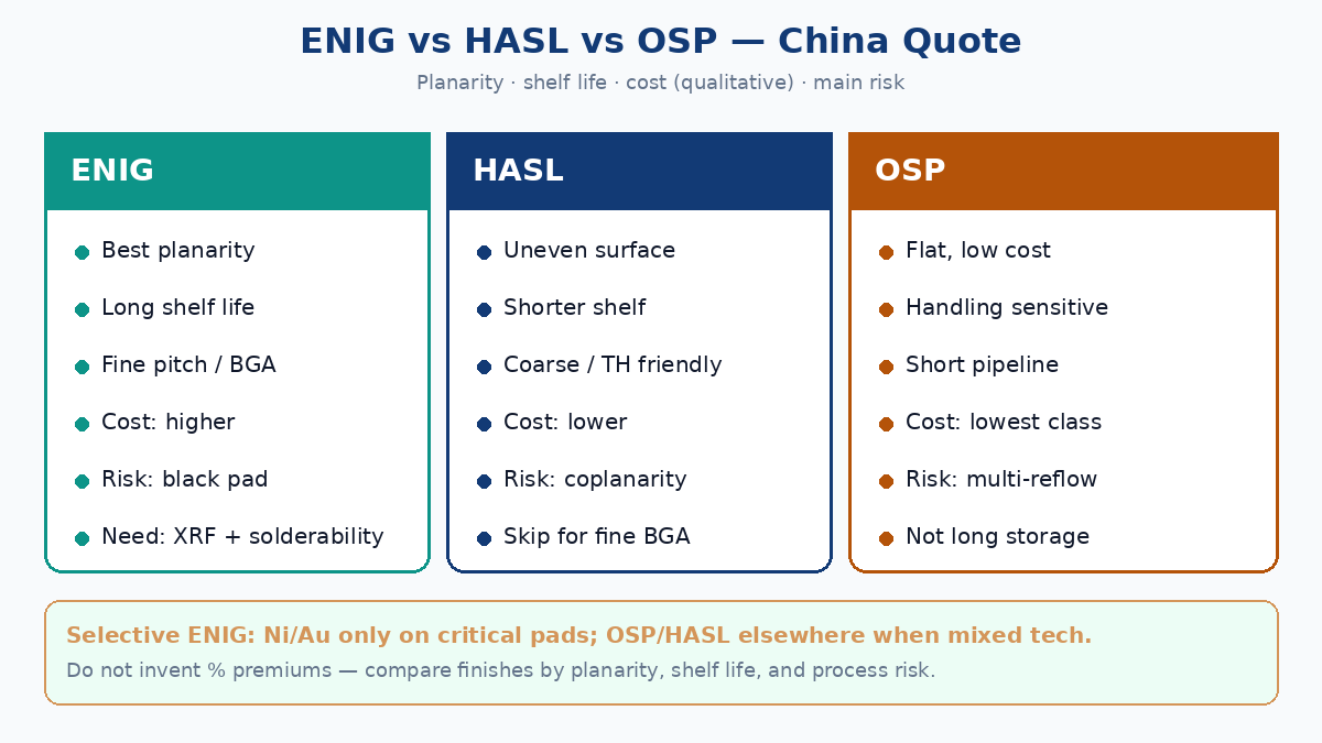
Use ENIG when fine pitch, BGA/QFN, multi-reflow, or shelf life drive the quote. Use HASL when through-hole / coarse pitch, short pipeline, and planarity is not critical — and you want the cheaper China line item. Do not pick ENIG “because gold sounds premium” on a HASL-friendly board.
ENIG vs OSP / ImAg / ENEPIG / hard gold
| Finish | When it wins | When ENIG still wins |
|---|---|---|
| OSP | Lowest cost, flat, short queue-to-assemble | Long storage, multi-reflow, rough handling |
| ImAg | Flat, mid cost, good solderability when fresh | Sulfur / humidity tarnish risk; longer shelf |
| ENEPIG | Wire bond + multi-reflow; palladium barrier vs Ni corrosion | Cost — only when Pd/wire-bond need is real |
| Hard gold (electrolytic) | Wear contacts, edge fingers, high mate cycles | Soldering surfaces — hard gold is the wrong solder finish |
ENEPIG is not “ENIG plus magic.” It adds palladium for specific bond/reliability needs and a higher cost stack. Hard gold is selective contact metallurgy — often with ENIG or OSP on solder pads (selective schemes), not a drop-in ENIG replacement everywhere.
Selective ENIG — mixed technology without paying for gold on every pad
Selective ENIG plates Ni/Au only where the drawing demands it (fine-pitch BGA lands, edge contacts that need ENIG class, keyed pads) while other copper uses OSP, HASL, or another finish behind mask/process separation.
Factory gain: lower gold area → lower metal/process cost; reliability where pitch and shelf life matter. Cost: mask/process complexity, clear zone drawings, and traveler discipline so the wrong finish does not land on BGA pads.
Call selective ENIG when the board mixes fine-pitch SMT + large TH / cheap copper areas, or when only connector/contact zones need gold-class surfaces. Silent “full board ENIG” on a mixed design is how quotes balloon without DFM benefit.
When to specify ENIG
Specify ENIG when one or more are true:
- Fine-pitch SMT / BGA / QFN where paste print planarity matters
- Multi-reflow lead-free assembly
- Long storage or international shipping before SMT
- High-reliability industrial / medical / aerospace-class wetting consistency (with Class notes elsewhere)
- Test pads / keypad contacts that need stable contact resistance without full hard-gold wear cycles
- Mixed tech where selective ENIG covers critical zones
Skip full-board ENIG when HASL or OSP meets pitch, storage, and reflow — and put the savings into stackup, impedance, or assembly yield instead.
Incoming QC checklist for buyers
Hand this to IQC / CM receiving with the packing list:
- Visual — uniform pale gold; no dark blotches, white residue, or obvious skip plate on pads/vias.
- XRF — Ni and Au on agreed pad features; Ni in 3–6 μm (rigid) window; Au per IPC-4552 statistical intent — keep records with the lot.
- Solderability — wetting or agreed aging method per PO; do not accept visual-only.
- Fab note match — finish callout on traveler equals drawing (full ENIG vs selective map).
- Packaging — dry pack / humidity control for long shelf; open-bag time rules if OSP zones exist on selective builds.
- Black-pad suspicion — non-wet pads with dark nickel under gold: quarantine, microsection / corrosion rating per fab capability — do not reflow “harder.”
- Over-gold watch — Au drifting high vs IPC-4552 window: cost and embrittlement risk; ask for process correction, not thicker gold as a fix.
What this post is — and what it is not
| Covered here | Not this article |
|---|---|
| ENIG definition, Ni+Au roles, process steps | Full surface-finish encyclopedia for every chemistry |
| IPC-4552 Ni/Au + XRF fab-note language | Invented embrittlement μm limits |
| Black pad as bath control + solderability acceptance | Brand bath recipes |
| ENIG vs HASL/OSP/ImAg/ENEPIG/hard gold (qualitative cost) | Percentage price tables |
| Selective ENIG + incoming QC checklist | Wire-bond process deep dive (ENEPIG territory) |
ENIG earns its premium when planarity, shelf life, and controlled nickel are the product — and when the fab note, XRF, and solderability gates make that premium measurable on a China quote.