
Boutique pedal builders do not lose sleep over “how to etch a board.” They lose units to hum, switch pop, pots that miss the enclosure holes, and small batches that sound different because footprints, finish, or grounding notes never made the China fab RFQ. An effect pedal PCB is the copper map that locks signal path, power, and mechanical hardware into one repeatable traveler. This factory note covers layout for low noise, DIY versus manufacture, the RFQ checklist that stops silent substitutions, the file pack PCBA actually needs, and the cost/lead-time drivers — without invented price tables.
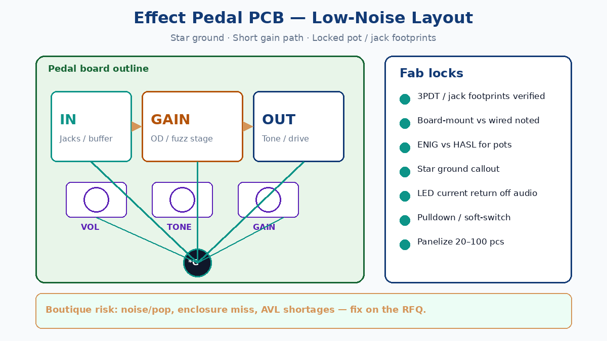
What an effect pedal PCB is
A guitar or instrument effect pedal PCB holds resistors, capacitors, semiconductors, pots, jacks, footswitches, and LEDs, and routes audio plus DC through copper instead of a rat’s nest of wires. On a working stompbox the board also carries mechanical truth: pot centers, jack heights, 3PDT body clearance, and LED hole position must match the drilled enclosure.
Three construction styles still show up in shops:
| Build style | When it helps | When it dies for production |
|---|---|---|
| Vero / stripboard / perf | Learning, one-off hacks | Trace errors, hard to clone, weak for board-mount pots |
| Point-to-point / hand wire | Vintage tone experiments | Labor, inconsistency, no Gerber trail for fab |
| Custom PCB | Any run that must sound the same twice | Needs DFM, footprint lock, and fab notes — or the fab invents defaults |
Once you sell more than a handful, custom PCB is the only path that CAM, stencil, and pick-and-place can repeat. The rest of this article assumes that path.
From schematic to fab-ready layout
Goal and mechanical envelope first
Name the effect class (fuzz, OD, delay, buffer), supply (usually 9 V center-negative; note 12/18 V if used), enclosure size, and whether pots/jacks/3PDT are board-mount or wired. Mechanical decisions before schematic save a full respin after the first dry-fit.
Schematic that survives translation
Use a verified topology or a redrawn known circuit with every net named. Label every R/C/diode/IC. Double-check transistor and op-amp pinouts. Add reverse-polarity protection and local decoupling on the schematic so they are not “forgotten” at layout.
Parts with footprints that match hardware
Boutique scrap often starts here: a 16 mm pot footprint drawn as 9 mm, a 3PDT library part that is not the switch you buy, or a DC jack that sits 1.5 mm too high for the enclosure. Prefer MPNs with stable AVL. Metal-film resistors and known op-amps (TL07x / NE5532 class) are fine — the factory cares more that the footprint and MPN agree than that you used a boutique brand.
Layout golden rules (shop-enforced)
- Route input → gain → tone → output in one direction; avoid looping the high-impedance input past the DC jack or LED.
- Use a star ground (or clearly partitioned analog / power returns that meet at one point). Do not share the LED return with the input ground pour.
- Decouple every IC (0.1 µF close; bulk 10–47 µF on the rail). Keep power traces short and away from the input node.
- Reverse-polarity diode and a small series resistor at the DC input are cheap insurance; omit them and field returns rise.
- Align pot, jack, and switch centers to the enclosure drawing at 1:1 before you release Gerbers.
DFM before you hit “order”
Typical China quick-turn rules for pedal boards (confirm on the quote): ~6/6 mil trace/space is comfortable; tighter needs a capability check. Annular rings must survive drill wander. Silk off pads. Polarity marks readable. Outline and copper clearances honest. Export Gerber + drill + BOM with MPNs — not a pretty PDF alone.
Prototype once, then freeze
Build one board, current-limit the supply, audio-probe stages, fix the layout once, then freeze revision for the 20–100 piece panel. Changing a pot footprint after panelization is how lead time doubles.
Noise and pop failure map (fab + assembly view)
Hobby guides say “use star ground.” Shops see the same failures across brands:
| Symptom | Usual root | What to put on fab / assembly notes |
|---|---|---|
| Hum / buzz | LED or power return sharing input ground; ground loop through chassis | Star ground; LED current loop off audio; note chassis bonding intent |
| Hiss / instability on fuzz/OD | Long high-Z input; gain stage next to DC jack wiring | Short input; keep first stage away from power entry; optional shield pour |
| Switch pop | No pulldown on input/output; hard true-bypass | Pulldown resistors; soft-switch / relay mute if design allows |
| Digital whine (delay/chorus) | Clock / DSP next to analog audio; shared return | Partition digital; separate returns; keep clock short |
| Intermittent crackle | Cold solder, flux residue, pot wiper noise on HASL whiskers | Clean flux; prefer ENIG on dense TH pot pads; inspect joints |
| Tone drift batch-to-batch | Footprint EQ, wrong finish, AVL substitute changing ESR/pinout | Lock footprints; AVL list; no silent “equiv OK” |
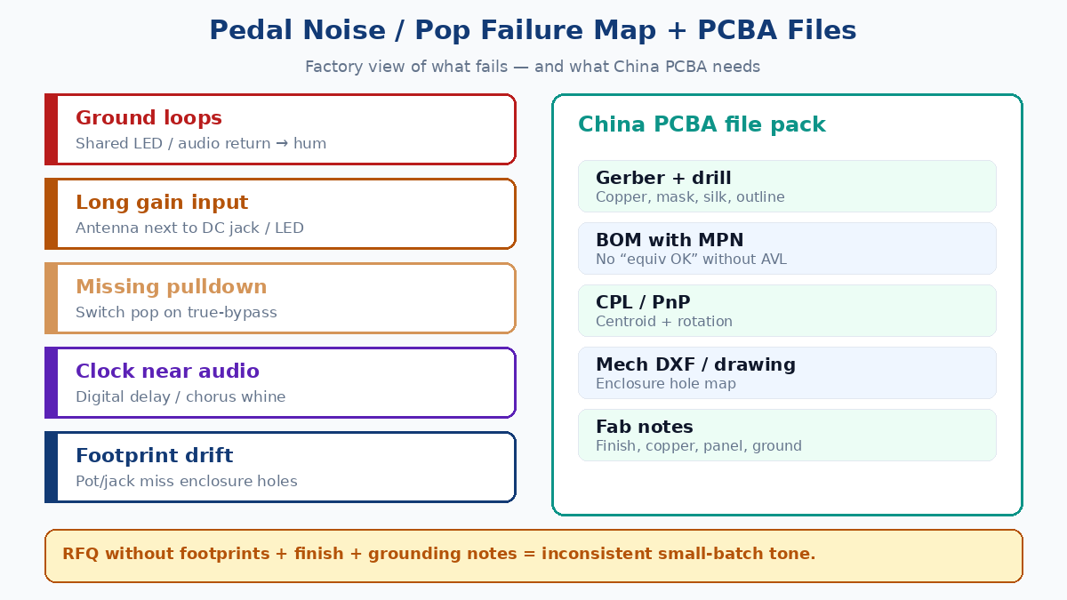
⚠️ Watch out: A board that “works on the bench” with flying wires can still fail in the enclosure when LED wires and DC jack share a ground path with the input. Dry-fit power and LED routing before you call layout done.
High-gain vs digital — constraints that kill yield
High-gain (fuzz / OD / distortion): CAM will not reject your art for “tone,” but assembly and test will. Long input stubs, missing pulldowns, and LED returns through the audio pour show up as noisy scrap or endless “sounds different” RMAs. Keep gain stages compact. Prefer board-mount pots to cut wire antennas. Do not run silk text over pot pads that need clean solder for wiper contact.
Digital / time-based (delay, chorus, modulation): Shops reject or yield-kill when (1) BGA/QFN pitch or via-in-pad exceeds the quoted process without VIPPO called, (2) clock crystals sit under noisy pours with no keepout, (3) mixed-voltage nets lack clear plane/return strategy, or (4) the BOM has no MPN for the DSP/codec and asks for “any equivalent.” Separate analog audio from digital islands. State layer count honestly — a squeezed 2-layer digital pedal often needs 4 layers for returns.
Buffers / boosters: Electrically simple, mechanically unforgiving. Input R/C must sit at the jack. One ground star. Enclosure misalignment on a one-knob buffer is still a full scrap event.
Tips by circuit type (compressed)
- Fuzz / OD: Short input, star ground, LED off audio, pulldowns, board-mount pots where possible.
- Delay / chorus: Isolate clock/DSP, split returns, decoupling per rail, keep converters away from jacks.
- Buffer / booster: Input network at jack, no ground loops, verify jack footprint height against enclosure.
DIY etch vs professional fab / PCBA
Toner-transfer or home etch is fine for single-sided experiments. It fails for plated vias, consistent copper, solder mask, and any batch that must match. Professional fab gives double-sided or multilayer boards, mask, HASL or ENIG, and optional SMT/TH assembly. For boutique runs, the decision is usually: prototype DIY or quick-turn bare board, then China PCBA once footprints and BOM AVL are frozen — not forever hand-soldering every unit.
RFQ / fab-note checklist for pedal boards
This is the list hobby articles skip and fabs need:
- Pot / jack / 3PDT footprint verification — library part vs the exact MPN you buy; include body outline and hole sizes.
- Board-mount vs wired — say which parts are soldered to the PCB and which fly on wires; CAM cannot guess.
- Surface finish — ENIG vs HASL: ENIG is kinder for repeated pot/switch soldering and dense TH pads; HASL is cheaper on simple boards. Write the choice; do not leave “default.”
- Copper weight / layers — most analog pedals are 1 oz 2-layer; digital or dense ground may need 4-layer. State it.
- Grounding notes — star ground intent, chassis lug, LED return path.
- Panelization for 20–100 pcs — V-score or tab-route, rail width, fiducials, tooling holes; ask for a panel drawing before mass etch.
- Silk and polarity — diode/LED/electrolytic marks that survive mask.
- RoHS / lead-free — assume lead-free unless you explicitly call tin-lead and the fab accepts it.
- Test expectations — bare-board E-test; assembled ICT/functional if you buy PCBA.
- AVL / no-sub list — especially germanium diodes, specialty FETs, and branded op-amps that define tone.
Phrases that stick:
- “ENIG; HASL not acceptable on pot/3PDT pads.”
- “Footprints locked to BOM MPNs for pots, jacks, 3PDT; no library substitution.”
- “Star ground as shown; LED cathode return not via input ground pour.”
- “Panelize for 50 pcs; provide panel drawing for approval.”
Phrases that do not stick:
- “High quality board” / “quiet layout” with no ground note
- “Any equivalent parts OK” on tone-critical semiconductors
- Enclosure hole positions only in a photo, not a DXF/drawing
Files China PCBA needs
| Deliverable | Why |
|---|---|
| Gerber + NC drill | Copper, mask, silk, outline — the fab language |
| BOM with MPN | Distributor-orderable part numbers; quantities; DNP called out |
| CPL / pick-and-place | Centroid X/Y, rotation, side — SMT cannot guess |
| Mechanical DXF or 2D drawing | Enclosure hole map vs pot/jack/LED/3PDT centers |
| Fab notes / stackup | Finish, copper, layer count, panel, grounding, special keepouts |
| Assembly drawing (nice to have) | TH orientation, wire lengths, torque-sensitive hardware |
Missing CPL stalls SMT. Missing mechanical drawing is how “perfect Gerbers” still miss the box holes. Missing MPN turns into AVL roulette and inconsistent tone.
Cost and lead-time drivers (no invented prices)
Quote math moves with:
- Layer count and copper weight — 4-layer and 2 oz cost more and sometimes queue longer than stock 2-layer 1 oz.
- Surface finish — ENIG above HASL; OSP rare on pedal TH work.
- Board size and panel utilization — odd outlines waste panel; ask for panel efficiency on 20–100 pcs.
- Min trace/space and via size — tightening below the house process adds capability surcharge or scrap risk.
- Parts AVL — long-lead ICs and specialty diodes dominate calendar time more than etch days; approve alternates in writing or accept wait.
- Assembly mix — SMT-only is faster than SMT + awkward TH pots/3PDT hand insert; design for process, not only for tone.
- Test depth — bare E-test vs powered functional test changes both price and escapes.
Lead time is not a fixed “3–5 days” slogan. Bare prototype on stock process can be days; PCBA waits on the slowest MPN and on your mechanical approval. Write finish, copper, panel, and AVL up front so the clock starts on a real traveler, not a clarification loop.
Assembly and test that lock tone
Clean joints, correct polarity, flux cleaned off high-Z nodes, and a dry-fit of pots/jacks before final solder. Add test points for rail and key audio nodes. Run a short play/burn-in on a known guitar/amp chain and record a revision note when anything changes. Consistency is the product; one heroic hand-wired prototype is not.
Related XFPCB guides
- PCB DFM: Design for Manufacturing Checklist Before You Order
- How PCB Assembly Works: From Gerber and BOM to Shipped Boards
- SMT vs DIP Assembly: When Each Process Fits Your Board