
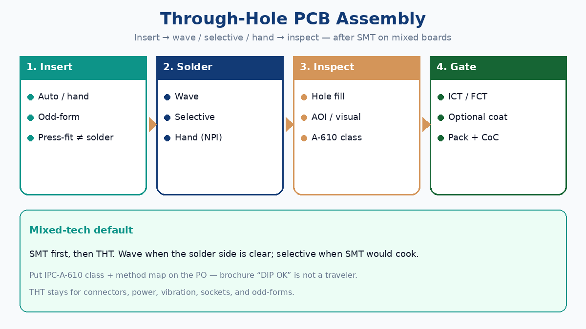
Through-hole technology (THT) did not disappear when SMT took over density. It stayed where mechanical anchors, high current, and vibration still beat surface pads: cable connectors that yank, power terminals that carry amps, tall magnetics and relays, and socketed parts that field techs must swap without a hot-air station. Modern China PCBA is usually mixed — SMT for ICs and passives, THT for the stress and power parts — and quotes fail when plants invent different wave versus selective maps, hole-fill classes, or insert sequences against the same BOM.
This guide answers first: when THT is still required on modern boards, the real process (insert → solder → inspect) and where it sits after SMT, a wave-versus-selective decision table with cost and DFM, IPC-A-610 Class 2 versus Class 3 hole-fill language buyers can put on a PO, the tools that matter for capability RFQs (inserters, selective, AOI — not brand fluff), and a China PCBA RFQ matrix that prevents quote surprises. SMT-vs-DIP decision depth lives on SMT vs DIP PCB assembly. End-to-end traveler context: how PCB assembly works.
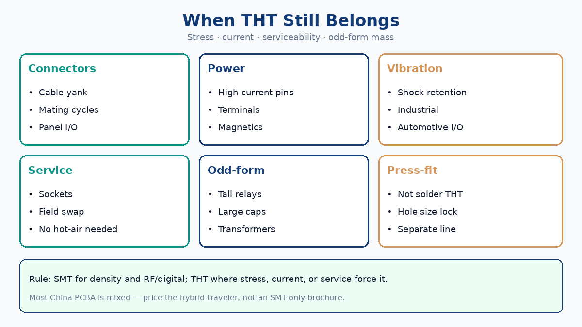
Answer first: when THT still belongs on modern boards
| Use case | Why THT wins | SMT-only risk if you force it |
|---|---|---|
| Panel / cable connectors | Pins anchored in plated holes resist yank and mating cycles | Pad peel, cracked fillets, intermittent opens |
| High-current power | Pin cross-section and barrel copper carry amps cleanly | Via farms and copper geometry stretch; thermal stress on pads |
| Vibration / shock | Mechanical retention through the board | Needs staking/underfill; still weaker under cable load |
| Field service / sockets | Replaceable modules without full SMT rework | Hot-air or BGA tools for every swap |
| Tall / odd-form parts | Transformers, large electrolytics, relays fit wave/selective/hand | Reflow profile wrong; tombstone or heat damage |
| Press-fit (related) | Controlled press — not solder THT | Mis-priced as “DIP insert” → scrap housings |
One-line rule: Default new digital and RF sections to SMT; keep THT where stress, current, serviceability, or odd-form thermal mass force it. Most production boards are hybrid — the RFQ must say so.
💡 Procurement Pro-Tip: List every THT refdes with intended solder method (wave / selective / hand / press-fit) before asking for unit price. “DIP capable” brochure lines do not make two China quotes comparable.
Related SMT stage detail: SMT PCB assembly process. Equipment vocabulary without brand theater: PCB assembly equipment list.
Process: insert → solder → inspect (after SMT on mixed tech)
THT on a traveler is three gateable steps — not a vague “DIP line.” On mixed boards, those steps run after SMT reflow so you do not wave-heat parts that have not been placed yet, and so you can plan adhesive or selective protection for already-soldered SMT.
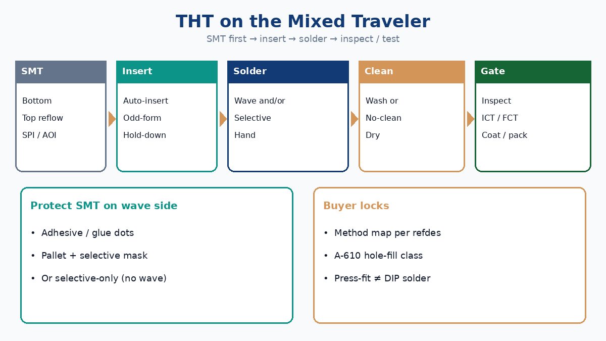
| Step | What the plant does | Buyer gate to write |
|---|---|---|
| 1. Insert | Auto-insert where pitch/packaging allows; semi-auto or hand for odd-forms; clinch/hold-down if needed | Pin count by insert class; odd-form list; press-fit called out separately |
| 2. Solder | Wave and/or selective and/or hand per pin class; flux and alloy per traveler | Method map per refdes; pallet/mask/adhesive yes-no; alloy (e.g. SAC305) |
| 3. Inspect | Visual / AOI on solder side; sample or 100% per class; X-ray only if nearby SMT warrants | IPC-A-610 class; hole-fill sample plan; first-article photos of densest THT zone |
Typical mixed order (confirm in writing): SMT bottom → SMT top → THT insert → wave/selective/hand → wash or no-clean → ICT/flying probe/FCT → optional coat → pack. Bottom-side SMT that must face a wave often needs adhesive or a process that never floods that side — selective is the usual escape. End-to-end gates: how PCB assembly works.
Press-fit is not step 2. Press-fit connectors need finished hole size, press equipment, and often no solder on those pins. Price them as their own line. Wave without a mask plan on press-fit neighborhoods creates bridges and cracked plastics.
⚠️ Watch Out for: Quotes that say “SMT + DIP OK” with no insert class, no solder-method map, and no inspect class. Two plants can both be capable and still deliver non-comparable prices and different hole-fill outcomes.
Wave vs selective: cost and DFM decision table
Wave floods the solder side; selective aims a nozzle or fountain at chosen pins. Hand bridges NPI and true odd-forms. Choose by pin density, nearby SMT, and scrap risk — not by which machine sounds more modern in a brochure.
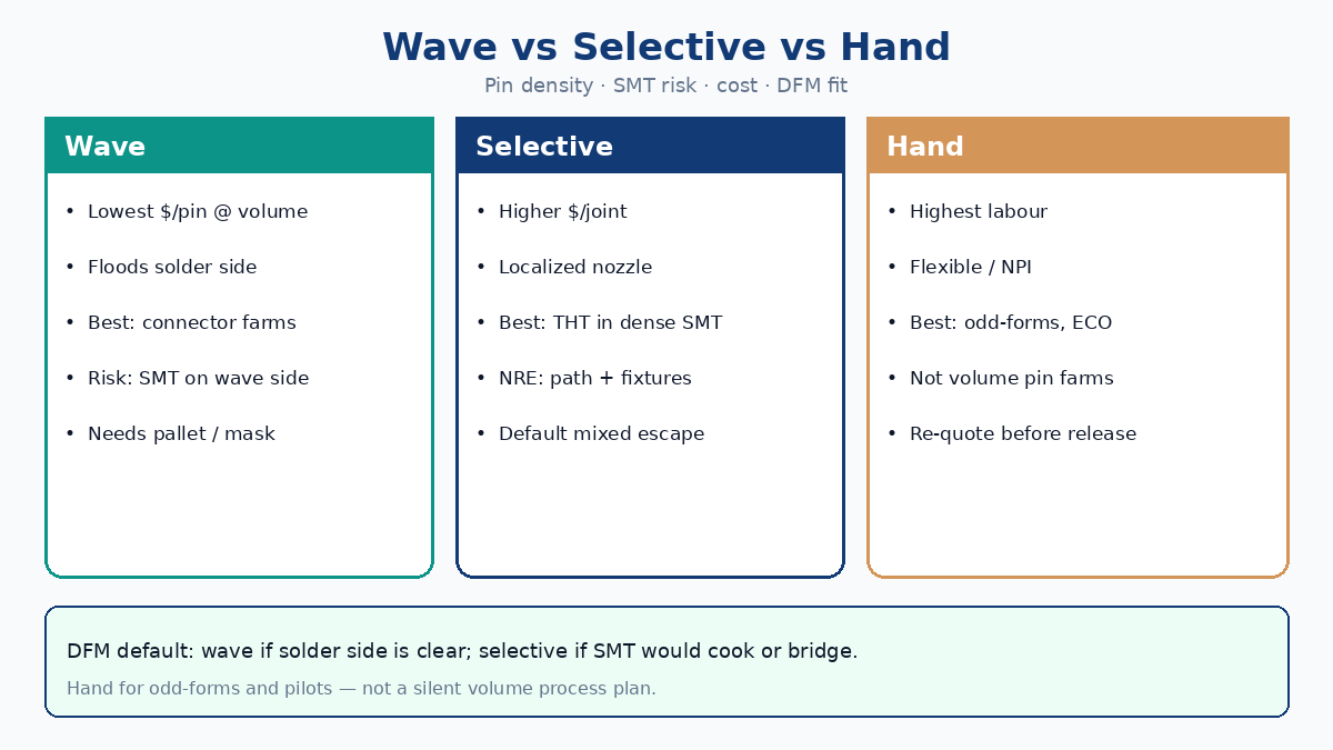
| Factor | Prefer wave | Prefer selective | Prefer hand |
|---|---|---|---|
| Pin count / density | Many pins, clear wave side, similar heights | Scattered THT among dense SMT; mixed heights | Few pins; ECO; prototype |
| Nearby SMT on solder side | Sparse or protected by pallet/mask/adhesive | Fine-pitch or tall SMT next to THT pins | Operator can avoid heat damage |
| Unit cost at volume | Lowest per pin when wave side is clean | Higher per joint; often lower scrap on mixed boards | Highest labour; not a volume plan |
| NRE / programming | Pallets, fixtures, wave profile | Path program + nozzles; fixture NRE | Minimal NRE; skill-dependent |
| Alloy / process mix | One alloy across the wave side | Easier localized control; mixed process windows | Flexible but inconsistent |
| DFM red flags | SMT too close to pins; fine THT pitch → bridges | Cannot reach shadowed pins; huge pin farms → slow | Production connector farms quoted as hand |
Practical default for China mixed PCBA: wave when the solder side is mostly THT connectors/power with keep-outs; selective when bottom or solder-side SMT would cook or bridge under a full wave; hand only for odd-forms and NPI — re-quote hand farms before volume release.
DFM habits that cut both cost and scrap
- Group THT on one side when layout allows.
- Keep paste-side and solder-side SMT clear of wave neighborhoods.
- Call out no-solder and press-fit holes on the assembly drawing, not only in a BOM cell.
- Demand who owns selective path NRE and pallet design on the quote.
- Tie hole-fill class to the densest connector neighborhood, not to a vague “IPC capable” line.
Method comparison also appears in the SMT-vs-DIP decision page; this table is the THT-process DFM view for RFQ marking. Companion: SMT vs DIP PCB assembly.
Hole-fill Class 2 vs Class 3 — buyer language (IPC-A-610)
Hole fill is an assembly acceptance topic under IPC-A-610, not a bare-board fab class under IPC-6012. Class 2 is the usual commercial/industrial default in China when the PO is silent. Class 3 tightens vertical fill and workmanship expectations on PTH joints — and raises rework and process-window cost. Put the class on the drawing and the PO, or you will get Class 2 habit with Class 3 hope.
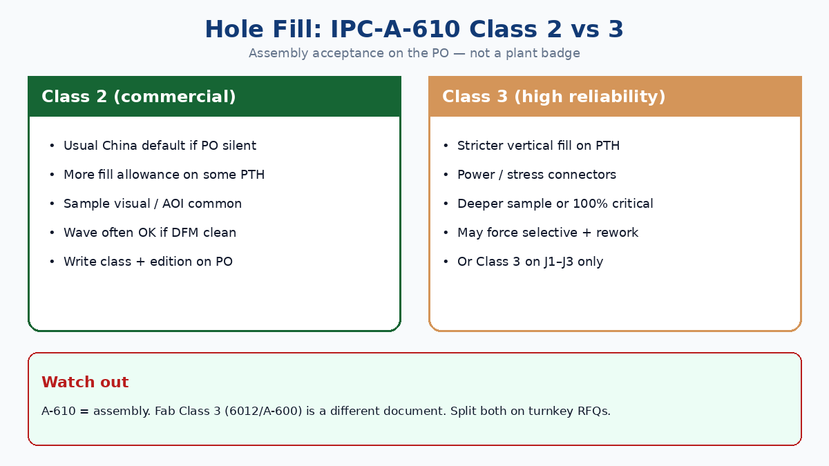
| Buyer need | Class 2 (typical commercial) | Class 3 (high reliability / safety-critical) | What to write on the PO |
|---|---|---|---|
| Vertical fill intent | More allowance for incomplete fill on some PTH joints (per cited A-610 edition) | Stricter vertical fill expectations on PTH | “IPC-A-610 Class X; edition YYYY” |
| Where it bites | Consumer/industrial I/O with known margin | Power, connectors under stress, long-life, safety | Optional: “Class 3 on J1–J3 only” |
| Inspection depth | Sample visual / AOI common | Deeper sample or 100% on critical joints; FA photos | Sample plan + FA photo of densest THT zone |
| Process impact | Wave often sufficient if DFM clean | May force selective, tighter flux/profile, more rework loops | Method map must support the class |
| Cost driver | Lower scrap allowance spend | Higher process control and potential rework | Do not Class-3 the whole board if only three connectors need it |
Buyer one-liner: Class is contractual acceptance, not a plant badge. “We do Class 3” without A-610 on the PO is marketing. Bare-board Class 3 (annular ring, plating) is a different document family — see IPC Class 3 PCB fabrication when fab class is also in scope.
⚠️ Watch Out for: Citing “IPC Class 3” with no document number, or putting A-610 Class 3 on a fab-only PO. Split fab class (6012/A-600) from assembly class (A-610) when both appear in one turnkey RFQ.
Tools that matter for RFQ capability (no brand fluff)
Capability questions should name process roles, not catalog logos. Brands change; the traveler does not.
| Tool role | What it proves on a THT job | Ask in the RFQ |
|---|---|---|
| Axial / radial / odd-form inserters | Auto-insert capacity vs hand-insert bottleneck | Max pin rate; which packages auto vs hand |
| Wave solder system | Volume pin flooding with pallets/masks | Pallet/mask available? Max board size? Alloy |
| Selective solder (nozzle/fountain) | Localized joints next to SMT | Path NRE owner; nozzles for your pin pitch |
| Press-fit press (if any) | Controlled force — not solder | Hole-size tolerance window; press tonnage class |
| Solder-side AOI / visual station | Hole-fill and bridge detection after THT | Coverage %; Class 2 vs 3 criteria loaded? |
| ICT / flying probe / FCT | Electrical proof after mixed solder | Fixture ownership; coverage rules |
Machine-by-machine context for the whole PCBA line: PCB assembly equipment list. Do not let a brand list replace the method map and class callouts above.
China PCBA RFQ matrix for through-hole (and mixed) jobs
Paste these fields so every bidder answers the same traveler. Brochure “DIP OK” fails here; comparable quotes survive.
| RFQ field | Why it matters | Example answer format |
|---|---|---|
| THT pin count by method | Drives insert + solder time and NRE | “90 wave; 16 selective; 3 hand odd-form; 0 press-fit” |
| Wave vs selective vs hand map | Makes unit prices comparable | Traveler mark-up per THT refdes |
| Hole-fill / IPC-A-610 class | Vertical fill and workmanship | “A-610 Class 2; Class 3 on J1–J2” |
| Mixed sequence | Heat budget and adhesive need | “SMT both sides → selective THT → no-clean → FCT” |
| Adhesive / pallet / mask | Double-sided mixed survival | “Glue bottom SMT” or “selective only — no wave” |
| Press-fit present? | Separate process, not solder THT | “Press-fit J4; finished hole per vendor PN” |
| Alloy + flux / wash | Stops SnPb-by-habit; coat compatibility | “SAC305; no-clean; wash if coat follows” |
| Inspect / test after THT | Coverage after mixed solder | “Solder-side AOI 100% connectors; flying probe NPI” |
| Selective / pallet NRE owner | Hidden cost and schedule | “Customer pays path NRE” or “included in setup” |
| Coat after solder? | Coat never before THT solder | “Conformal coat after wash/dry; keep-outs on drawing” |
Also attach: BOM lines flagged THT vs SMT, CPL for SMT, assembly drawing with polarity and keep-outs, and whether the kit is turnkey or consignment (connectors are often long-lead). Sourcing model depth: full turnkey vs consignment PCB assembly when that page is in your set; otherwise lock kit ownership on line 1 of the RFQ.
Design habits that keep THT quotes honest
- Flag every THT and press-fit refdes on the assembly drawing.
- Size pads and holes for the stated A-610 class before RFQ.
- Keep SMT clearances around wave neighborhoods.
- Re-quote hand-soldered pilots before volume — pin-minutes on a bench are not a process plan.
- Demand first-article solder-side photos of the densest THT zone plus the sample plan tied to class.
Soft next step
If you already have Gerbers, BOM, and an assembly drawing, send the THT refdes list with a draft wave/selective/hand map and the A-610 class you intend to enforce. XFPCB can mark method and hole-fill expectations against a China mixed-tech traveler — without assuming a full wave that would cook bottom-side SMT — and return which RFQ rows above belong on your quote. Pair this page with SMT vs DIP, how PCB assembly works, PCB assembly equipment list, and SMT PCB assembly process when decision, traveler, tools, and SMT stages need one story.