
The quote said "full SMT assembly" and listed AOI. The purchase order closed. First articles looked clean under a camera. Three months later, field returns clustered on one BGA: cold balls and head-in-pillow that no optical station could see. The shop had no SPI on the traveler, and the reflow oven ran a generic paste-datasheet recipe with no thermocouple board for that panel. Unit price was never the failure -- missing process gates were.
This article is a China PCBA walkthrough of the SMT PCB assembly process for overseas procurement managers and technicians: what surface mount actually is versus through-hole, how a controlled line moves from paste print through reflow and test, which station catches which defect, and which RFQ clauses separate a profiled line from marketing fluff. It is the line process and parameter pack -- not a density pitch and not a partner-scoring scorecard.
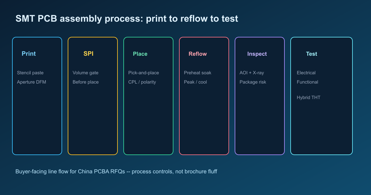
SMT versus THT for buyers who write RFQs
Surface-mount technology places components on copper pads with solder paste, then forms joints in a reflow oven. Parts stay on the surface; both sides of the board can carry active and passive loads when sequence and thermal mass are planned. Through-hole technology inserts leads through plated holes and solders them by wave, selective solder, or hand iron. PTH joints win on mechanical retention for large connectors, transformers, and high-stress interfaces.
Modern commercial boards are hybrid more often than pure. Passives, ICs, BGAs, and QFNs run SMT first. Press-fit or wave/selective through-hole parts usually come after reflow so the SMT joints are already formed. When a quote says "SMT only" but your BOM still has pin headers and power terminals, ask which station solders the through-hole -- and when it sits relative to reflow -- before you compare cycle time.
For buyers, the distinction that matters is not a textbook definition. It is which packages on your BOM force SPI, profiled reflow, and X-ray, and which force a second process after SMT.
Walk the line: what each station catches and what it cannot
Solder paste printing
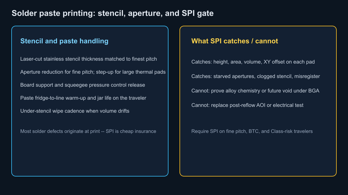
A stainless stencil sits over the board. A squeegee forces paste through apertures onto pads. Yield on fine pitch is dominated by stencil thickness, aperture reduction, board support, and paste condition -- not by the printer model name on a brochure.
Practical notes China lines actually enforce: match stencil thickness to the finest pitch on the panel; use step-up or step-down foils when large thermal pads and 0201/0402 passives share a side; control paste warm-up from refrigerator to line and track open time on the jar; set under-stencil wipe cadence when SPI volume starts to drift. Via-in-pad and BTC center-pad aperture design decide void risk later -- print geometry is not a lab footnote.
Catches early: wrong paste volume, gross misregister, clogged apertures that starve pads. Cannot catch: wrong alloy chemistry if the jar was mislabeled, future head-in-pillow from coplanarity, or a BGA ball that will open under vibration weeks later.
SPI before placement
Solder paste inspection measures height, area, volume, and XY offset on each pad after print and before parts land. Industry process studies commonly attribute a large share of SMT solder defects to the print step -- often cited in roughly the 30% to 60%+ range depending on product mix. The exact percentage matters less than the cost curve: a print miss fixed at SPI is a reprint; the same miss after reflow is scrap, rework, or a field return.
SPI without response rules is theater. Define out-of-window actions and feed repeating signatures back into stencil DFM. Require SPI in the RFQ for fine pitch, BGA/QFN/LGA, and Class 2 / Class 3 risk travelers. Prototype jobs sometimes waive SPI after the paste window is proven -- waive it in writing so quotes stay comparable.
Pick-and-place
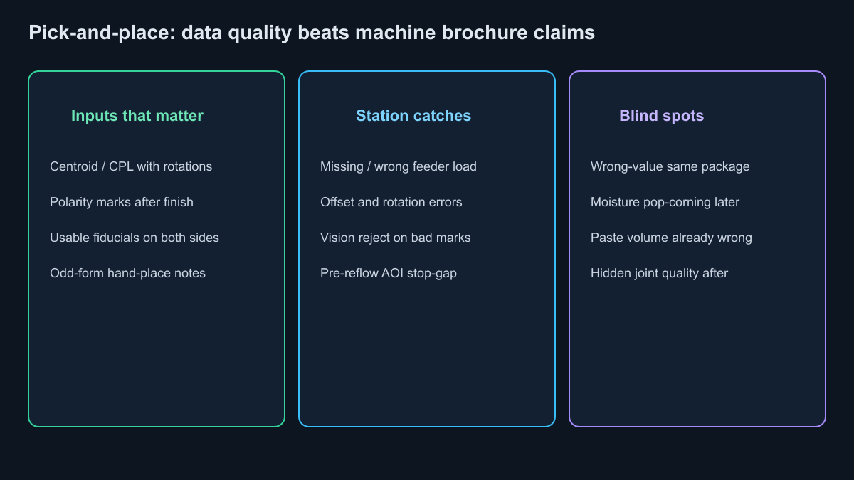
High-speed placers pull parts from feeders and set them on paste. Machine capability matters, but NPI failures more often come from data: bad CPL rotations, polarity marks that disappear after finish, unusable fiducials, and odd-form parts with no hand-place note on the same revision package.
Catches: missing parts, feeder mix-ups that vision can flag, offset and rotation when programs and fiducials are sound. Pre-reflow AOI can stop obvious placement errors before solder forms. Cannot catch: a wrong-value resistor in the same package outline if marks were never checked, moisture damage that appears only as pop-corning in reflow, or paste volume that was already wrong upstream.
Reflow soldering
The panel moves through a controlled oven. Paste activates, reaches liquidus, wets pads and terminations, then solidifies on cool-down. This is the metallurgical yield lever for the whole SMT side.
AOI after reflow
Automated optical inspection compares the board to CAD or a golden sample. It catches missing and misaligned parts, polarity errors, tombstones, bridges, and many visible fillet issues on exposed leads and chips. Hard limit: joints under package bodies are outside the camera view. AOI can confirm a BGA is present and roughly seated; it does not inspect the balls underneath.
Selective X-ray
X-ray reads density under BGA, QFN, LGA, and other bottom-terminated packages. Use it for voids, opens, bridges, and head-in-pillow. Equipment time makes coverage selective by risk unless Class 3 or field history demands wider sampling. Inspect is not test: a clean X-ray image does not prove the circuit boots.
Electrical and functional test
Flying probe fits prototypes and moving layouts (minutes per board, no bed-of-nails fixture). ICT fits frozen designs with test-point access and stable volume (seconds per board, fixture NRE). Functional test powers the product under near-use conditions. Wrong values, high-resistance joints, and firmware/interface faults live in this layer -- not in AOI alone.
Reflow profiling as the yield lever
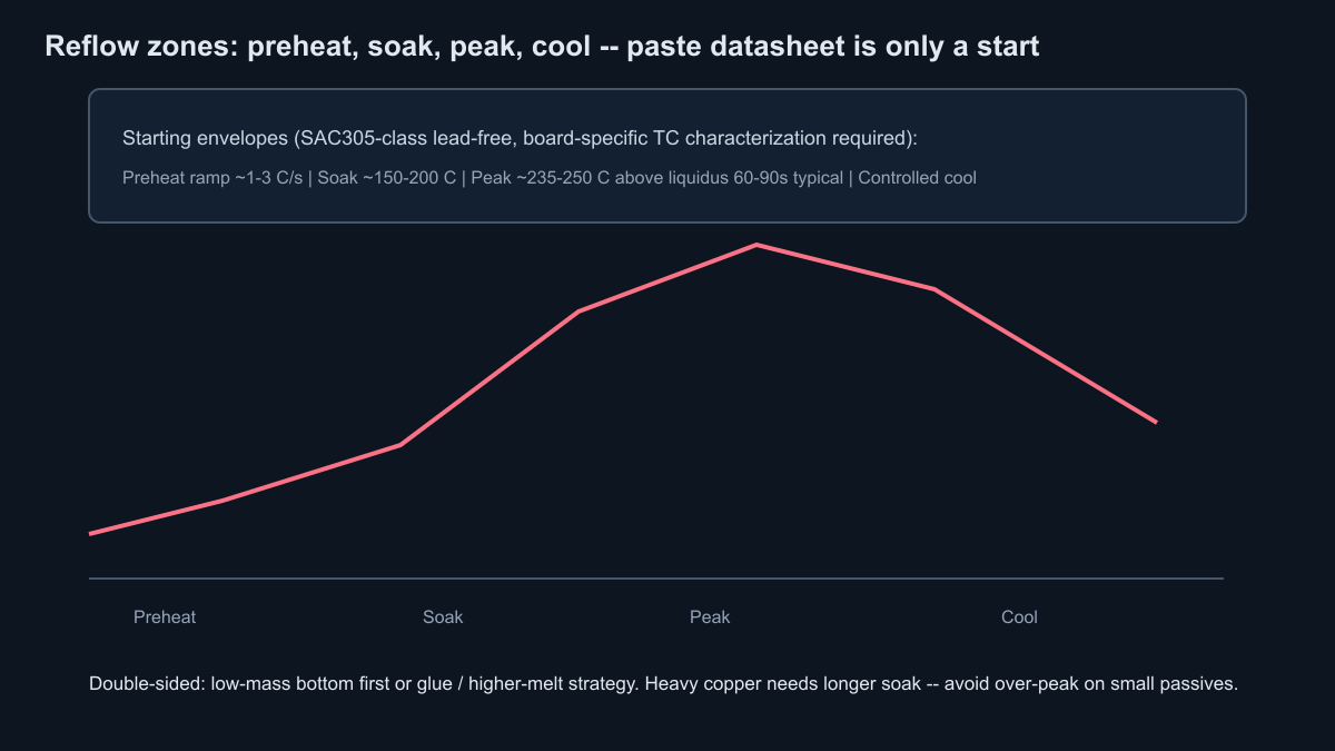
Paste supplier envelopes are starting points, not finished profiles. A serious line runs a thermocouple board that matches your copper mass, layer count, and package mix, then locks a profile to that characterization.
Zone logic buyers should recognize:
- Preheat: controlled ramp (commonly on the order of 1-3 C/s for many lead-free pastes) to drive off volatiles without shocking small parts.
- Soak / activation: time in the flux-active window (often roughly 150-200 C for SAC305-class pastes) so surfaces wet evenly across heavy and light thermal masses.
- Peak: above liquidus long enough for wetting (many programs target roughly 235-250 C peak with about 60-90 s above liquidus) without cooking sensitive packages.
- Cool: controlled cool-down for grain structure and to limit tombstoning from uneven solidification.
Double-sided assemblies need a sequence plan: typically the lower-mass or lower-risk side first, or adhesive / higher-melt strategies so bottom parts do not fall or re-melt out of control on the second pass. Heavy-copper and large ground pours need longer soak; the same peak that wets a big thermal pad can over-stress nearby 0402s if the profile was never measured on your stackup.
If the quote cannot show a first-article profile plot for your board, treat "we follow the paste datasheet" as an incomplete answer.
Defect map: symptom back to the earlier step
When AOI or X-ray flags a defect, procurement still needs a root-station story -- otherwise every lot becomes random scrap.
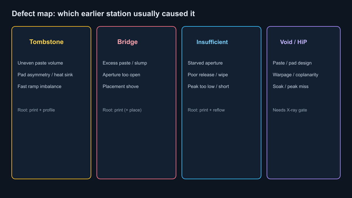
- Tombstone: uneven paste volume on the two pads, pad copper asymmetry that sinks heat differently, or a ramp that melts one side first. Usually print geometry plus profile, not "the placer was angry."
- Bridge: excess paste, slump after print, aperture too open for pitch, or placement that shoves paste into the gap. Start at stencil and SPI windows.
- Insufficient / open fillet: starved aperture, poor release, wipe neglect, or peak time/temperature too short. Print and reflow share blame; placement alone rarely invents missing volume.
- Voiding and head-in-pillow under BTC: aperture and pad design, paste and outgassing, board/package warpage, and soak/peak that never fully coalesced the ball to the pad. Optical AOI will not close this; X-ray and profile characterization will.
Mapping defects to stations turns RFQ language into process control instead of a machine shopping list.
Hybrid builds: selective or wave after SMT
Connectors, transformers, and tall through-hole parts usually enter after SMT reflow. Selective solder hits discrete PTH sites with less thermal shock to nearby SMT. Wave solder still appears on high PTH density when fixtures and masking protect SMT zones. Hand solder remains for odd-form and low volume when automation NRE will not amortize.
RFQ clarity: state whether THT is selective, wave, or hand; whether SMT is complete and inspected before PTH; and whether press-fit replaces solder on mechanical interfaces. A "full SMT" line item that silently omits your PTH connectors is a schedule slip waiting for a change order.
Prototype versus volume: when flying probe, ICT, and X-ray belong in the RFQ
Prototype and NPI: AOI plus flying probe, SPI when fine pitch or paste risk is real, selective X-ray on hidden packages, light functional bring-up. Skip ICT fixture NRE while the layout still spins.
Stable volume: inline SPI and AOI, expanded or sampled X-ray for BGA/QFN populations, ICT once test points and design freeze exist, functional test full or sampled by risk.
Make X-ray mandatory in the RFQ whenever the BOM includes bottom-terminated packages that can fail in the field without optical evidence -- especially fine-pitch BGA on Class 2 / Class 3 or vibration-exposed products. Waive it only with eyes open and in writing.
RFQ clause pack: documents and process evidence
Give the factory a complete package so quotes price the same traveler:
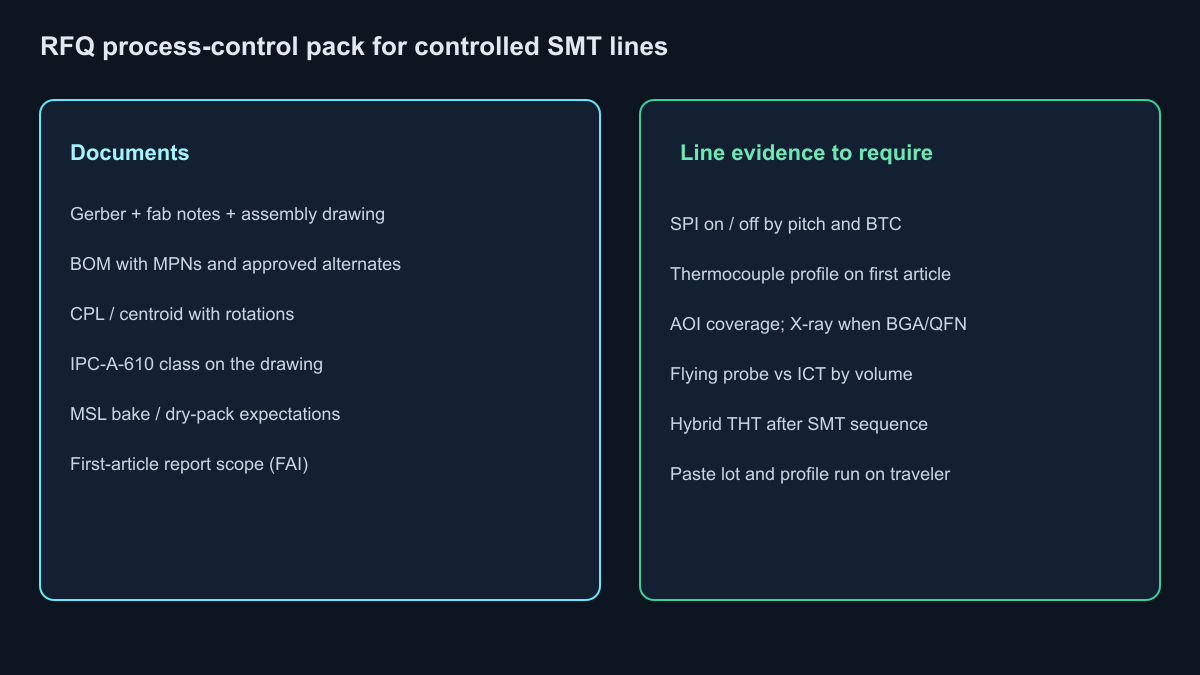
- Gerbers, fab notes, and assembly drawing with IPC-A-610 class stated (add J-STD-001 soldering expectations when the program requires them).
- BOM with manufacturer part numbers and approved alternates; no "or equivalent" without a signed alternate path.
- CPL / centroid with rotations and reference designators that match the drawing revision.
- Moisture-sensitivity handling: MSL levels, bake rules, and dry-pack expectations for humidity-sensitive parts.
- Process gates: SPI required or waived by pitch/package; AOI pre- and/or post-reflow; X-ray coverage for named BTC packages; flying probe versus ICT versus functional test scoped as line items.
- First-article expectations: profile plot for the panel, SPI/AOI summary, sample X-ray images for BGA pitch when applicable, paste lot and machine IDs on the traveler.
A shop that can answer those clauses with artefacts is running a controlled line. A shop that answers only with machine brand photos is selling capacity, not process.
SMT in PCBA is a chain of print, inspect, place, reflow, inspect again, and test -- with through-hole work often after. Yield disasters and schedule slips shrink when RFQs name SPI, board-specific reflow profiles, package-matched X-ray, and the hybrid sequence your BOM actually needs. The first article that includes those records is cheaper than the field return that proves they were missing.