
No single PCB design program wins every job. Pick by board complexity, team process, and budget -- then judge the tool by the manufacturing package it can export, not by the logo on the splash screen. From the China fab chair, clean Gerber or ODB++/IPC-2581, NC drill, stackup/fab drawing, pick-place, BOM, and netlist matter more than whether you drew the board in KiCad, Altium Designer, OrCAD X, Allegro X, Fusion 360 Electronics / EAGLE, or DipTrace. This guide compares those suites for overseas EE and procurement, maps decision paths by role, lists what every RFQ must include, and flags the handoff failures that stall CAM -- without treating specialized semiconductor/PI tools (Ansys RedHawk-class rail analysis) as day-to-day layout suites.
What China fabs care about when you name an EDA tool
Fabs care that your release package is complete, revision-locked, and unambiguous -- not which PCB design software logo appears in the project file.
CAM builds from manufacturing outputs. A tidy Altium project that ships a wrong layer map still holds. A KiCad board with a complete Gerber set, drill table, stackup note, and pick-place usually runs. Treat the EDA choice as a workflow and license decision for your team; treat the release package as the contract with the fab.
DRC is not DFM. Passing the tool's design-rule check only proves you met the rules you typed into that tool. Fab DFM adds process windows: etch yield, min annular ring, NPTH vs PTH, mask dams, impedance coupons, via fill, and assembly clearances. Ship both a DRC report and fab-facing notes.
Procurement Pro-Tip: Accept designs from any major EDA suite if the release package is complete. Do not shortlist vendors by "we only take Altium." Shortlist by whether CAM can open a locked rev of Gerber/ODB++, drill, fab drawing, CPL, BOM, and netlist without guessing.
PCB design software compared: KiCad through Allegro X
Use this qualitative table to shortlist -- then verify export settings on a real board before you freeze the AVL for layout tools.
| Tool | Best for | Strength | Watch-outs | Manufacturing export readiness |
|---|---|---|---|---|
| KiCad | Hobby, education, cost-sensitive NPI | Full schematic-to-PCB flow; strong community libraries; no seat tax for solo work | Team vault / formal PLM is DIY; library discipline is on you | Gerber, drill, IPC-2581/ODB++ paths mature when you configure layers carefully; document the layer map |
| Fusion 360 Electronics / EAGLE class | Mech+elec co-design, makers, light commercial | CAD/ECAD integration; fast for mechatronic enclosures | Complex high-layer / high-speed teams often outgrow it | Solid Gerber/drill for conventional boards; confirm stackup and fab-drawing extras on dense jobs |
| DipTrace | Small teams wanting a simple paid schematic/PCB suite | Approachable UI; practical for 2-6 layer product boards | Ecosystem and high-speed feature depth thinner than big suites | Gerber/drill/pick-place workable; still verify NPTH and layer names on first China RFQ |
| Altium Designer | Pro product teams, multi-board, managed libraries | Strong schematic/PCB/library/ECO flow; common in commercial OEMs | Seat cost is vendor-quoted (typically subscription or enterprise quote); process overhead if over-configured | Excellent Gerber/ODB++/IPC-2581 and fab docs when release scripts are locked; bad outputs still possible if layer pairs are wrong |
| OrCAD X | Cadence-centric schematic shops, mixed Allegro handoff | Familiar Capture-class schematic; X-platform updates | Layout depth vs Allegro depends on the exact product seat | Good manufacturing exports when the release checklist is enforced; align units and layer map early |
| Allegro X | Enterprise high-speed / high-rel / large teams | Constraint-driven layout; scales to dense high-layer work | Learning curve and license model (vendor-quoted / enterprise) | Strong for controlled fab packages; still needs human fab notes and stackup table |
Seat prices are not published here as XFPCB facts -- ask the EDA vendor. Specialized semiconductor power-integrity / rail tools in the Ansys RedHawk class are not substitutes for these layout suites; use them when you have die/package PDN problems, not for everyday FR-4 board drafting.
Decision paths: which PCB design program fits your team
Match the tool to complexity and process maturity, then lock an export checklist before the first China fab RFQ.
1. Hobby / education / one-off prototypes
Choose KiCad or a light Fusion/EAGLE-class flow when boards are 2-4 layers, budgets are tight, and one engineer owns the project. Export Gerber + drill + a one-page fab note (thickness, finish, copper weight). Do not skip NPTH callouts just because the board is "simple."
2. Startup / NPI with a few paid seats
Choose KiCad with strict library rules, DipTrace, or Fusion 360 Electronics / EAGLE when you need speed and light BOM control. Escalate to Altium Designer when you need managed components, multi-board, or frequent ECO with contract layout houses. Freeze a release script early so every spin uses the same Gerber layer map.
3. Professional product team (shipping SKUs)
Choose Altium Designer or OrCAD X (with layout depth that matches your Cadence seat) when revision control, library governance, and assembly outputs are weekly work. Demand ODB++ or IPC-2581 plus classic Gerber as a backup, pick-place, and a fab drawing with stackup. Treat "DRC clean" as necessary but not sufficient.
4. Enterprise high-speed / high-reliability
Choose Allegro X (or Altium with strong constraint and length-match process) when you run dense BGAs, controlled impedance, and formal ECO. Pair layout with the right SI/PI analysis for the interface -- not a semiconductor RedHawk-class rail tool unless you truly have package/die PDN scope. Budget for vendor-quoted licenses and trained owners of the constraint file.
What every tool must export for a China fab RFQ
Every major EDA path must produce the same manufacturing contract -- formats differ, content does not.
Minimum release package:
- Copper artwork -- Gerber (RS-274X) or ODB++ / IPC-2581, with a written layer map (Top Copper, Inner1, etc.)
- NC drill -- plated vs non-plated holes called out; slots and back-drill noted if used
- Fab drawing / stackup -- layer count, copper weights, dielectric/Tg, board thickness, finish, mask/silk, impedance targets with reference layers
- Pick-place (CPL) -- centroids, rotations, side, refdes aligned to the BOM rev
- BOM -- manufacturer MPN, refdes, DNP lines, and approved alternates where allowed
- Netlist -- for assembly/test correlation and ECO checks
- Notes -- outline tolerances, via fill, edge plate, gold fingers, UL marks, specials
Common handoff failures that burn RFQ time
Most CAM holds come from package mistakes, not from "wrong" EDA brands.
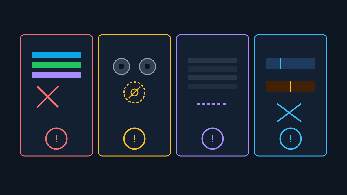
- Wrong layer map -- Top copper labeled as silk, or inner layers swapped; CAM etches the wrong intent.
- Missing NPTH -- mounting holes plated by accident; screws short to copper or press-fit fails.
- No stackup -- impedance and thickness become shop guesses; quotes are not comparable.
- Imperial / metric mix -- outline in mm, drill in inches, or library lands mismatched to BOM text.
- Library footprint errors -- wrong pitch, mirror, or pin-1; first article fails before fab yield is even relevant.
- DRC-only release -- no fab notes for finish, via fill, or mask dams; CAM invents defaults you did not want.
Watch Out for: Zipping "all outputs" from the EDA without opening the zip. Confirm every Gerber opens, drill tool sizes match the fab drawing, and NPTH holes are marked. A green DRC light does not prove the zip is fab-ready.
Related XFPCB guides
- PCB Board Design and Layout Considerations -- placement order, return paths, fiducials, and pre-order layout checks
- PCB DFM: Design for Manufacturing -- why DRC-clean boards still draw CAM questions
- How PCBs Are Made -- fab process steps that your export package must feed
- Multilayer PCB Stackup Fabrication Guide -- stackup tables and reference planes CAM can build